
Portfolio 2014 | Carlos García Muñoz | Architecture & Landscape Architecture
Beehive: an FPGA-based multiprocessor architecture Master’s Degree in Information Technology final thesis
Oriol Arcas Abella
February 2, 2009 – September 13, 2009
BSC-CNS Facultat d’Informàtica de Barcelona Universitat Politècnica de Catalunya
i
Abstract
In recent years, to accomplish with the Moore's law hardware and software designers are tending
progressively to focus their efforts on exploiting instruction-level parallelism. Software simulation
has been essential for studying computer architecture because of its flexibility and low cost.
However, users of software simulators must choose between high performance and high fidelity
emulation. This project presents an FPGA-based multiprocessor architecture to speed up
multiprocessor architecture research and ease parallel software simulation.
ii
Acknowledgements
This project wouldn’t have been possible without the invaluable help of many people. First of all, I
would like to thank Nehir Sönmez, the other beekeeper of the team, for his contributions to this
project and for being constant at work but maintaining his great sense of humor.
I would like to thank also Professors Adrián Cristal and Osman Unsal, co-directors of this thesis, for
their good advises and expertise guiding this project. And also the rest of the people at the BSC –
MSR centre, for making live there a little bit happier and easier.
I have to mention also Professor Satnam Singh, for his honest interest and valuable experience
about FPGAs, and Steve Rhoads, the author of Plasma, who always answered our questions about
his designs.
Finally I would like to thank the FIB staff and professors for their dedication and help with the
project’s procedures.
iii
Contents
Abstract .......................................................................................................................................... i
Acknowledgements.........................................................................................................................ii
Contents ........................................................................................................................................ iii
List of figures ................................................................................................................................. vi
List of tables ................................................................................................................................ viii
List of listings ................................................................................................................................. ix
1 Introduction ......................................................................................................................... 10
1.1 Background and motivation ...................................................................................... 10
1.2 Objectives ................................................................................................................. 10
1.3 State of the art.......................................................................................................... 11
1.4 Introducing the BSC .................................................................................................. 13
1.5 Planning .................................................................................................................... 13
1.6 Outline ..................................................................................................................... 14
2 FPGA, HDL and the BEE3 platform ........................................................................................ 16
2.1 FPGA: the computation fabric ................................................................................... 16
2.1.1 Technology ........................................................................................................... 16
2.1.2 FPGA-based system design process ....................................................................... 18
2.1.3 Applications .......................................................................................................... 18
2.2 Hardware Description Languages .............................................................................. 19
2.2.1 Hierarchical designs .............................................................................................. 20
2.2.2 Wires, signals and registers ................................................................................... 21
2.2.3 Behavioral vs. structural elements ........................................................................ 22
2.3 FPGA CAD tools ......................................................................................................... 22
2.4 The Berkeley Emulator Engine version 3 ................................................................... 24
2.4.1 Previous multi-FPGA systems ................................................................................ 24
2.4.2 Previous BEE versions ........................................................................................... 25
2.4.3 BEE version 3 ........................................................................................................ 26
2.4.4 The BEE3 DDR2 controller ..................................................................................... 28
3 MIPS and the RISC architectures ........................................................................................... 31
iv
3.1 MIPS, the RISC pioneers ............................................................................................ 31
3.1.1 Efficient pipelining ................................................................................................ 32
3.1.2 A reduced and simple instruction set .................................................................... 34
3.1.3 Load/Store architecture ........................................................................................ 35
3.1.4 Design abstraction ................................................................................................ 35
3.1.5 An architecture aware of the memory system ....................................................... 36
3.1.6 Limitations ............................................................................................................ 36
3.2 The MIPS R3000 processor ........................................................................................ 37
3.3 RISC processors as soft cores .................................................................................... 38
4 Plasma, an open RISC processor ........................................................................................... 40
4.1 Plasma CPU ............................................................................................................... 40
4.2 Plasma system .......................................................................................................... 42
4.3 Memory mapping ..................................................................................................... 43
4.4 Why CP0 is so important ........................................................................................... 44
4.5 Differences with R3000 ............................................................................................. 45
5 The Honeycomb processor ................................................................................................... 47
5.1 Coprocessor 0 ........................................................................................................... 47
5.2 Virtual memory ......................................................................................................... 49
5.2.1 Virtual memory regions......................................................................................... 50
5.2.2 TLB hardware ........................................................................................................ 51
5.2.3 TLB registers and instructions ............................................................................... 53
5.2.4 The translation process ......................................................................................... 54
5.2.5 Memory mapping ................................................................................................. 56
5.3 Exception handling ................................................................................................... 57
5.3.1 Interruption mechanism ....................................................................................... 58
5.3.2 Interruption and exception registers ..................................................................... 59
5.3.3 TLB exceptions ...................................................................................................... 60
5.3.4 Returning from interruptions ................................................................................ 60
5.4 Operating modes ...................................................................................................... 61
6 The Beehive multiprocessor system ..................................................................................... 62
6.1 Beehive architecture ................................................................................................. 62
6.2 Honeycomb, the Beehive processor .......................................................................... 63
6.3 The bus state machines............................................................................................. 64
7 Conclusions .......................................................................................................................... 67
7.1 Analysis and results .................................................................................................. 67
7.2 Future work .............................................................................................................. 70
7.3 Personal balance ....................................................................................................... 70
8 References ........................................................................................................................... 71
9 Appendix A: processor registers ........................................................................................... 74
10 Appendix B: instruction set architecture ............................................................................... 75
10.1 Nomenclature ........................................................................................................... 75
v
10.2 Arithmetic Logic Unit ................................................................................................ 75
10.3 Shift .......................................................................................................................... 76
10.4 Multiply and divide ................................................................................................... 76
10.5 Branch ...................................................................................................................... 76
10.6 Memory access ......................................................................................................... 77
10.7 Special instructions ................................................................................................... 77
vi
List of figures
Figure 1: Gantt diagram of the project. ........................................................................................ 14
Figure 2: 4-input lookup table. ..................................................................................................... 17
Figure 3: 8 to 1 multiplexer (a), implementation with LUT4 elements (b) and implementation with
LUT6 elements (c). .................................................................................................................. 17
Figure 4: FPGA-based design flow. ............................................................................................... 18
Figure 5: VHDL hierarchical structure. .......................................................................................... 20
Figure 6: Xilinx ISE screenshot. ..................................................................................................... 23
Figure 7: Xilinx ChipScope Pro Analyzer screenshot. ..................................................................... 23
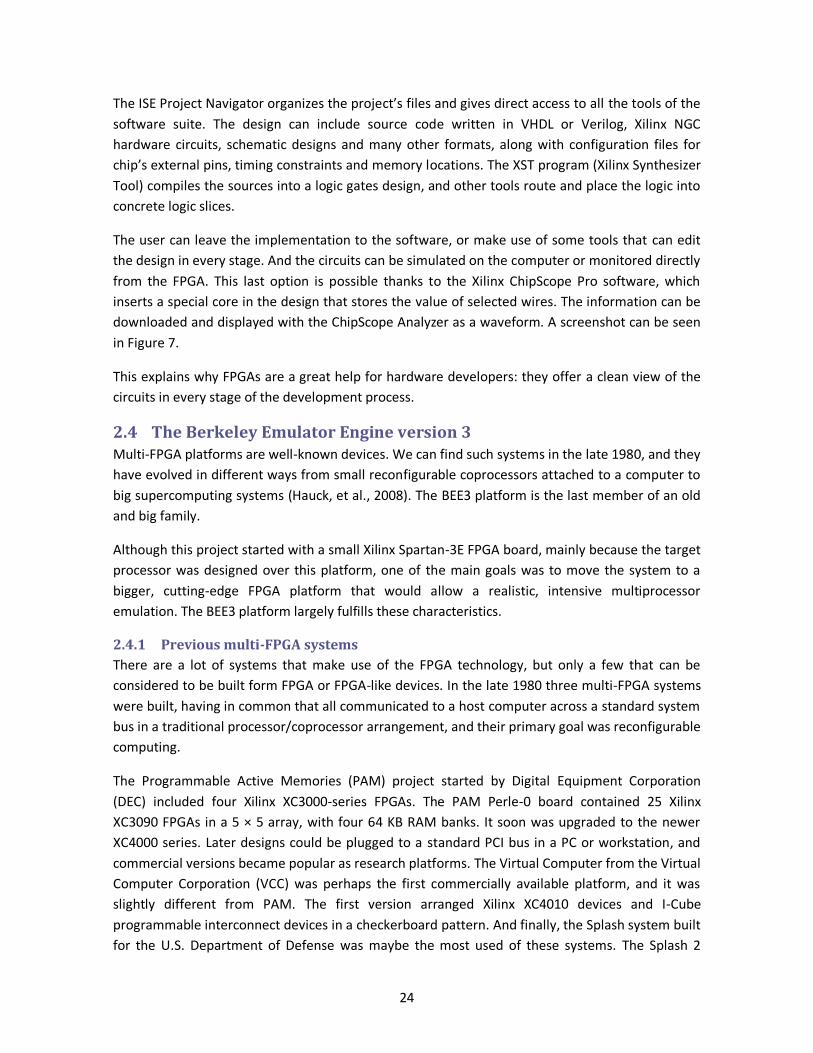
Figure 8: BEE system. ................................................................................................................... 26
Figure 9: BEE interconnection network. ....................................................................................... 26
Figure 10: BEE2 system. ............................................................................................................... 26
Figure 11: BEE2 architecture. ....................................................................................................... 26
Figure 12: BEE3 main PCB subsystems. ......................................................................................... 27
Figure 13: BEE3 DDR controller data and address paths. .............................................................. 29
Figure 14: TC5 block diagram. ...................................................................................................... 30
Figure 15: classical instruction execution flow. ............................................................................. 32
Figure 16: ideally pipelined execution flow. .................................................................................. 33
Figure 17: instructions with different execution time can cause delays in the execution flow. ...... 33
Figure 18: MIPS instruction types. ................................................................................................ 35
Figure 19: the R3000 functional block diagram. ............................................................................ 37
Figure 20: the 5-stage R3000 pipeline. ......................................................................................... 38
Figure 21: Plasma CPU block diagram. .......................................................................................... 41
Figure 22: Plasma pipeline. .......................................................................................................... 41
Figure 23: Plasma subsystems. ..................................................................................................... 42
Figure 24: aligned accesses (a) and unaligned accesses (b). .......................................................... 45
Figure 25: block diagram of the Honeycomb CPU. ........................................................................ 48
Figure 26: data path of a MTC0 instruction................................................................................... 49
Figure 27: example of the virtual and physical mappings of two processes. .................................. 50
Figure 28: MIPS memory mapping. .............................................................................................. 51
Figure 29: Honeycomb pipeline. ................................................................................................... 51
Figure 30: data path of a Honeycomb address translation. ........................................................... 52
vii
Figure 31: Xilinx CAM core schematic symbol. .............................................................................. 52
Figure 32: TLB hardware blocks. ................................................................................................... 53
Figure 33: EntryLo, EntryHi and Index registers. ........................................................................... 53
Figure 34: TLB address translation flowchart. ............................................................................... 55
Figure 35: comparison between Plasma and Honeycomb memory mappings. .............................. 57
Figure 36: Status register. ............................................................................................................ 59
Figure 37: Cause register. ............................................................................................................. 59
Figure 38: BadVAddr register. ...................................................................................................... 60
Figure 39: Beehive architecture.................................................................................................... 63
Figure 40: Beehive bus request life cycle. ..................................................................................... 64
Figure 41: Bus client bus-side and processor-side FSMs. ............................................................... 65
Figure 42: Beehive bus arbiter FSM. ............................................................................................. 66
Figure 43: Beehive intercommunication schema. ......................................................................... 66
Figure 44: slice logic utilization. .................................................................................................... 68
Figure 45: block RAM utilization. .................................................................................................. 68
Figure 46: FPGA logic distribution with 4 Plasma cores. ................................................................ 69
Figure 47: Dhrystone 2 benchmark results. .................................................................................. 69
viii
List of tables
Table 1: soft processor designs. ................................................................................................... 12
Table 2: Plasma memory mapping. .............................................................................................. 43
Table 3: Honeycomb data paths. .................................................................................................. 49
Table 4: Honeycomb memory mapping. ....................................................................................... 57
Table 5: exception cause codes. ................................................................................................... 59
Table 6: MIPS CPU registers. ........................................................................................................ 74
Table 7: MIPS CP0 registers. ......................................................................................................... 74
Table 8: integer arithmetic instructions. ....................................................................................... 76
Table 9: shift instructions. ............................................................................................................ 76
Table 10: integer multiplication and division instructions. ............................................................ 76
Table 11: branch instructions. ...................................................................................................... 77
Table 12: memory access instructions. ......................................................................................... 77
Table 13: special instructions. ...................................................................................................... 77
ix
List of listings
Listing 1: VHDL program for the “inhibit” gate. ............................................................................. 21
Listing 2: Verilog program for the “inhibit” gate. .......................................................................... 21
Listing 3: load delay slot. .............................................................................................................. 34
Listing 4: programming a random TLB entry. ................................................................................ 54
Listing 5: VHDL code that checks addresses correctness in Honeycomb. ....................................... 56
Listing 6: interruption service VHDL code. .................................................................................... 58
Listing 7: Plasma assembler code for returning from an interruption............................................ 60
Listing 8: TLB code for throwing and returning from interruptions. .............................................. 61
10
1 Introduction
The current document is the final thesis of the Master’s Degree in Information Technology of the
Barcelona School of Informatics (FIB) at the Technical University of Catalonia (UPC). The system
presented was proposed by and developed at the Barcelona Supercomputing Center.
1.1 Background and motivation Historically, computer architects have depended on the growing number of transistor per die to
implement a single large processor that is able to work at increasing frequencies. But continued
performance gains from improved integration technologies are becoming increasingly difficult to
achieve due to fundamental physical limitations like heat removal capacity and quantum tunneling
(Zhirnov, et al., 2003). In recent years, to accomplish with the Moore's law hardware and software
designers are tending progressively to focus their efforts on exploiting instruction-level
parallelism. Typical microprocessors include two or more cores and it is expected that a large
number of it will be available soon (Seiler, et al., 2008).
However, this situation has brought two major problems. On one hand, it seems that software
cannot take profit of the possibilities that technology is offering. Programs have poor parallelism
and only small solutions like transactional memory have been presented. Likewise, the problems
associated with designing ever-larger and more complex monolithic processor cores are becoming
increasingly significant (Matzke, 1997). Among other difficulties that slow innovation in these
fields, there is a key concept: testing and simulation.
Traditionally, software simulation has been essential for studying computer architecture because
of its flexibility and low cost. Regrettably, users of software simulators must choose between high
performance and high fidelity emulation. Whatever it is a new multiprocessor architecture or a
transactional memory library, software simulators are orders of magnitude slower than the target
system and don't offer realistic conditions for the testing environment.
1.2 Objectives This project aimed to design and implement an FPGA-based multiprocessor architecture to speed
up multiprocessor architecture research and ease parallel software simulation. This system had to
11
be a flexible, inexpensive multiprocessor machine that would provide reliable, fast simulation
results for parallel software and hardware development and testing.
Performance wasn’t a priority because the system would be used as a fast academic simulator, not
an end-user product that would compete with commercial solutions. It wouldn’t be wrong if it was
orders of magnitude slower than real hardware, but it should be orders of magnitude faster than
software.
Based on FPGA technology, the system had to provide the basic components of a multiprocessor
computer like a simple but complete processor, a memory hierarchy and minimal I/O. From this
point, while software could be tested under a real multiprocessor environment adapted to the
user needs, the platform would also allow researching in computer architecture.
The motivation of this project came from the research in transactional memories, and the initial
objective was to include support for hardware transactional memory. This mechanism, understood
as an improvement of a traditional coherency system, was the first application of the system but a
secondary objective subject to the development of a basic multiprocessor system. As explained in
the planning section, it couldn’t be implemented during the development of this work and will be
done after the end of this project becoming out of the scope of this thesis.
There were two full-time students dedicated to this project. This quantity can be considered small
given the expertise of the team in the hardware development field and really small compared to
similar projects. Thus, an implicit objective of the project was to produce an inexpensive system,
limiting the system characteristics to the time and resources available.
1.3 State of the art From the beginning it was clear that BEE3 would be the developing platform for this project. The
developers of that machine and the previous versions have been working in computer architecture
research in a project called Research Accelerator for Multiple Processors (RAMP), born from the
collaboration of six universities, in special the University of California at Berkeley, and some
prominent companies like Intel, Xilinx, IBM and Microsoft (University of California, 2009). The
objectives of the RAMP project were similar to the ones pursued by this work. Their research has
produced impressive and innovative designs that explore software and hardware simulation, like
ProtoFlex, HAsim and FAST, and the different colors of RAMP: RAMP White, a parallel functional
model to simulate parallel systems in a FAST simulator; RAMP Gold, a SPARC-based manycore
system; RAMP Blue, a message-passing multiprocessor; and so on.
But there was no clear candidate among their designs that would fit the requirements of this
project. Among other reasons:
Most of the designs were not implemented in the BEE3 platform.
The systems were designed having in mind performance and not the amount of FPGA logic
resources. For example, RAMP Blue project used 21 BEE2 modules to implement up to
1008 cores, and RAMP Gold uses 8 BEE3 modules.
12
The processors chosen were commercial products that didn’t have any source available,
like Xilinx MicroBlaze.
Since 2008 the project has produced little research, and it is difficult to know if the
subprojects are being adapted to the new BEE3 platform or unfortunately have been
discontinued.
Another project of interest is at the moment only a brief mention in a report of the BEE3 authors
(Davis, et al., 2009). Created by Chuck Thacker, very similar not only for the time it was started and
its characteristics, but also because it shares the same name with the system presented here,
“Beehive”, by the time this project is ending there are no news about its status. Unfortunately the
author of the current document knew about that project a few months after beginning this work,
but in the future maybe an interesting synergy can appear between both projects.
Once decided that a new platform would be build, the first part of the project consisted in an
initial research about FPGA technology and a RISC processor that would fit the requirements of the
future system. It was recommendable an open design that could be easily modified without
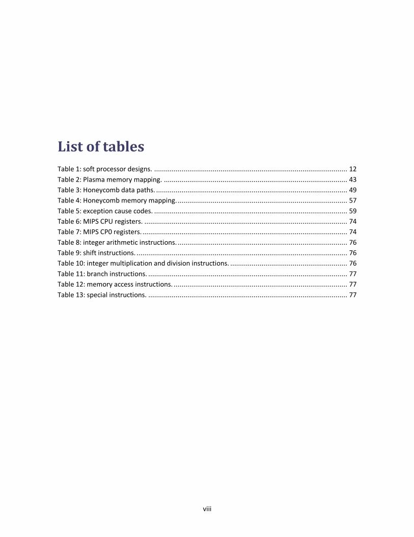
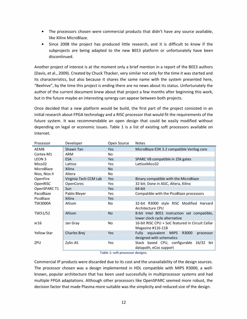
depending on legal or economic issues. Table 1 is a list of existing soft processors available on
Internet.
Processor Developer Open Source Notes
AEMB Shawn Tan Yes MicroBlaze EDK 3.2 compatible Verilog core Cortex-M1 ARM No LEON 3 ESA Yes SPARC V8 compatible in 25k gates Mico32 Lattice Yes LatticeMico32 MicroBlaze Xilinx No Nios, Nios II Altera No OpenFire Virginia Tech CCM Lab Yes Binary compatible with the MicroBlaze OpenRISC OpenCores Yes 32-bit; Done in ASIC, Altera, Xilinx OpenSPARC T1 Sun Yes 64-bit PacoBlaze Pablo Bleyer Yes Compatible with the PicoBlaze processors PicoBlaze Xilinx Yes TSK3000A Altium No 32-bit R3000 style RISC Modified Harvard
Architecture CPU TSK51/52 Altium No 8-bit Intel 8051 instruction set compatible,
lower clock cycle alternative xr16 Jan Gray No 16-bit RISC CPU + SoC featured in Circuit Cellar
Magazine #116-118 Yellow Star Charles Brej Yes Fully equivalent MIPS R3000 processor
designed with schematics ZPU Zylin AS Yes Stack based CPU, configurable 16/32 bit
datapath, eCos support Table 1: soft processor designs.
Commercial IP products were discarded due to its cost and the unavailability of the design sources.
The processor chosen was a design implemented in HDL compatible with MIPS R3000, a well-
known, popular architecture that has been used successfully in multiprocessor systems and had
multiple FPGA adaptations. Although other processors like OpenSPARC seemed more robust, the
decision factor that made Plasma more suitable was the simplicity and reduced size of the design.
13
1.4 Introducing the BSC This project has been developed in the Barcelona Supercomputing Center – Centro Nacional de
Supercomputación, a research center of the Technical University of Catalonia (UPC) at Barcelona.
In 1991 the European Center for Parallelism of Barcelona (CEPBA) started its activities gathering
the experience and needs from different UPC departments. The Computer Architecture
Department (DAC), one of the top 3 computer architecture departments in the world (according to
BSC-CNS) provided experience in computing, while other five departments interested in
supercomputing joined the center. Inheriting the experience of CEPBA, BSC-CNS was officially
constituted in April 2005 sponsored by the governments of Catalonia and Spain.
BSC-CNS manages MareNostrum, one of the most powerful supercomputers of Europe designed
by IBM and dedicated not only to non-computer calculations for Life Sciences and Earth Sciences,
but also to supercomputing architectures and techniques research. When MareNostrum was built
in 2005, it was the most powerful supercomputer of Europe and one of the most powerful of the
world. In 2006 doubled its calculation capacity, becoming again the most powerful of Europe. BSC-
CNS, which manages the Spanish supercomputing network, will probably return to the top
positions with MareIncognito, a ground-breaking supercomputer that will replace MareNostrum
with its around 100 times more calculation capacity.
This project was developed at the Computer Architecture for Parallel Paradigms department, in
collaboration with Microsoft Research.
1.5 Planning The duration of this project was 6 months, starting from February 2009. The delivering date was in
September, so the implementation could be extended to the end of July and the writing of the
thesis could be done in August.
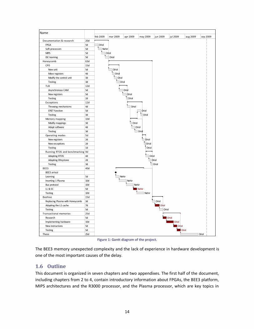
The work presented here has been developed in coordination with Nehir Sönmez, a PhD student
from BSC. The parts developed by each member of the team are clearly shown in the Gantt
diagram of Figure 1: while I, Oriol Arcas, modified the Plasma to add virtual memory support and
other features, Nehir unveiled the secrets of BEE3 and implemented an initial version of the
multiprocessor system.
As the months passed, it became clear that the last parts of the project (colored in red in the Gantt
diagram) weren’t unaffordable and I spent the last days of the project finishing the multiprocessor
bus system initially sketched by Nehir.
14
Figure 1: Gantt diagram of the project.
The BEE3 memory unexpected complexity and the lack of experience in hardware development is
one of the most important causes of the delay.
1.6 Outline This document is organized in seven chapters and two appendixes. The first half of the document,
including chapters from 2 to 4, contain introductory information about FPGAs, the BEE3 platform,
MIPS architectures and the R3000 processor, and the Plasma processor, which are key topics in
15
this project. The second half, from chapters 5 to 7, covers the description of the project and the
implementation details of the system that was developed.
After this first introduction chapter, chapter 2 describes what FPGAs are, their possible
applications and the tools used to program it in this project. Then there is a small description of
hardware description languages, and a brief introduction to the history of FPGAs systems and the
BEE platform. At the end the BEE3 architecture is presented with some other related topics like its
DDR controller design.
Chapter 3 is dedicated to RISC architectures, specially the MIPS designs and the architecture used
in this project, the MIPS R3000 processor. This chapter helps to understand why RISC processors
are a good choice to be emulated in an FPGA and to be used as the processing element in a
multiprocessor system.
Chapter 4 describes the Plasma processor, an open design compatible with R3000 and designed as
a soft core. It is compared to the original R3000 architecture, revealing some of its limitations like
not having the coprocessor number 0.
Chapter 5 introduces the Honeycomb processor, the new design developed in this project that
extends and improves the Plasma processor. Changes include the development of the coprocessor
0, which provides virtual memory and exception handling support, and a modification of the
memory mapping.
Chapter 6 exposes the Beehive multiprocessor system. Beehive can coordinate an arbitrary array
of Honeycomb processors through a centralized bus protocol.
Chapter 7 includes the conclusions of the document, and the future work that can be done with
the system presented in this work. The appendixes contain detailed information about the
registers of the processor and the instruction set that is supported.
16
2 FPGA, HDL and the BEE3 platform
This project is entirely designed to run on an emulation engine based on reconfigurable logic
technology. Recent years, FPGA devices have evolved rapidly, offering new possibilities and
techniques that make available a whole new range of computing paradigms. FPGA enthusiasts
expect that in the upcoming years there will be a significant growth in this field as it is becoming
more and more popular and given that FPGA, unlike microprocessors, maybe can turn increasing
die area and speed into useful computation (Chang, et al., 2005).
2.1 FPGA: the computation fabric In computer electronics, there are two ways of performing computations: hardware and software.
An application-specific integrated circuit (ASIC) provides highly optimized devices, in means of
space, speed and power consumption; but it cannot be reprogrammed and requires an expensive
design and fabrication effort. Software is flexible, but it is orders of magnitude slower than ASIC
and limited to hardware characteristics.
Field-programmable gate arrays (FPGA) include benefits from both hardware and software, as it
implements computation like hardware (spatially, across a silicon chip) and can be reconfigured
like software: it is a semiconductor device that can be reconfigured after manufacturing. It
contains an array of logic blocks that can perform from simple logic functions like AND and XOR to
complex combinations, like small finite state machines. These blocks are interconnected with
dynamic networks that can be programmed as well. Modern FPGAs also include specialized blocks
such as memory storage elements or high speed digital signal processing circuits.
2.1.1 Technology
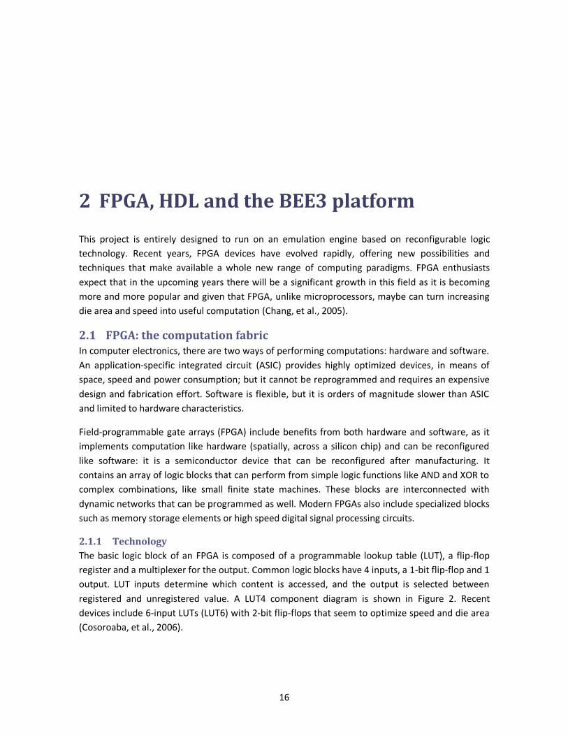
The basic logic block of an FPGA is composed of a programmable lookup table (LUT), a flip-flop
register and a multiplexer for the output. Common logic blocks have 4 inputs, a 1-bit flip-flop and 1
output. LUT inputs determine which content is accessed, and the output is selected between
registered and unregistered value. A LUT4 component diagram is shown in Figure 2. Recent
devices include 6-input LUTs (LUT6) with 2-bit flip-flops that seem to optimize speed and die area
(Cosoroaba, et al., 2006).
17
Figure 2: 4-input lookup table.
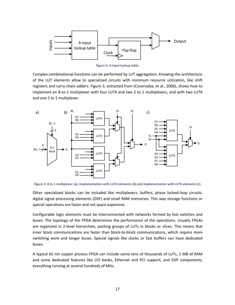
Complex combinational functions can be performed by LUT aggregation. Knowing the architecture
of the LUT elements allow to specialized circuits with minimum resource utilization, like shift
registers and carry-chain adders. Figure 3, extracted from (Cosoroaba, et al., 2006), shows how to
implement an 8-to-1 multiplexer with four LUT4 and two 2 to 1 multiplexers, and with two LUT6
and one 2 to 1 multiplexer.
Figure 3: 8 to 1 multiplexer (a), implementation with LUT4 elements (b) and implementation with LUT6 elements (c).
Other specialized blocks can be included like multiplexers, buffers, phase locked-loop circuits,
digital signal processing elements (DSP) and small RAM memories. This way storage functions or
special operations are faster and not space expensive.
Configurable logic elements must be interconnected with networks formed by fast switches and
buses. The topology of the FPGA determines the performance of the operations. Usually FPGAs
are organized in 2-level hierarchies, packing groups of LUTs in blocks or slices. This means that
inner block communications are faster than block-to-block communications, which require more
switching work and longer buses. Special signals like clocks or fast buffers can have dedicated
buses.
A typical 65 nm copper process FPGA can include some tens of thousands of LUTs, 1 MB of RAM
and some dedicated features like I/O banks, Ethernet and PCI support, and DSP components;
everything running at several hundreds of MHz.
S2
LUT4
LUT4
LUT4
LUT4
S1 S0
D7 D6
D5 D4
D3 D2
D1 D0
O 8:1
MUX D0…7
S0…2
3
O 8
b) c)
S2
D7
S0
D6 D5 D4
S1 LUT6
LUT6 D3 D2 D1 D0
O
a)
4-input lookup table In
pu
ts
Flip-flop Clock
Output
18
2.1.2 FPGA-based system design process
The FPGA customizing process can be simplified to storing the correct values to memory locations.
This is similar to compiling a program and loading it onto a computer: the creation of an FPGA-
based circuit design is a simple process of creating a bitstream to load into the device.
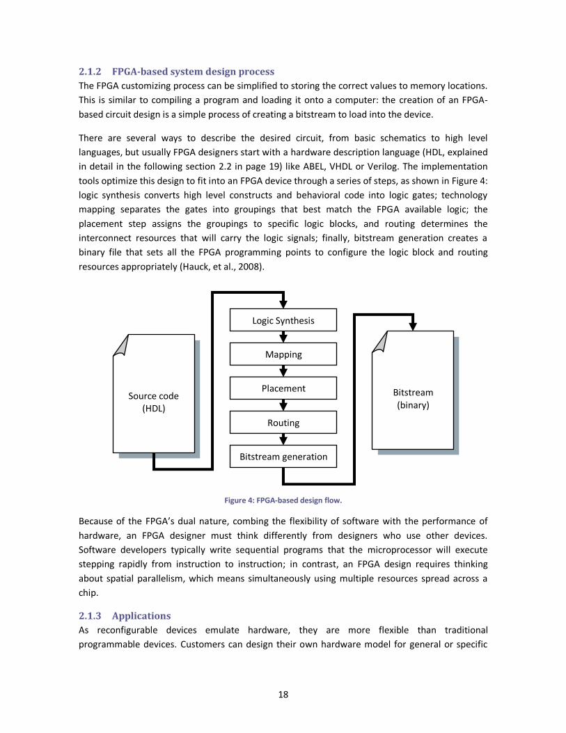
There are several ways to describe the desired circuit, from basic schematics to high level
languages, but usually FPGA designers start with a hardware description language (HDL, explained
in detail in the following section 2.2 in page 19) like ABEL, VHDL or Verilog. The implementation
tools optimize this design to fit into an FPGA device through a series of steps, as shown in Figure 4:
logic synthesis converts high level constructs and behavioral code into logic gates; technology
mapping separates the gates into groupings that best match the FPGA available logic; the
placement step assigns the groupings to specific logic blocks, and routing determines the
interconnect resources that will carry the logic signals; finally, bitstream generation creates a
binary file that sets all the FPGA programming points to configure the logic block and routing
resources appropriately (Hauck, et al., 2008).
Figure 4: FPGA-based design flow.
Because of the FPGA’s dual nature, combing the flexibility of software with the performance of
hardware, an FPGA designer must think differently from designers who use other devices.
Software developers typically write sequential programs that the microprocessor will execute
stepping rapidly from instruction to instruction; in contrast, an FPGA design requires thinking
about spatial parallelism, which means simultaneously using multiple resources spread across a
chip.
2.1.3 Applications
As reconfigurable devices emulate hardware, they are more flexible than traditional
programmable devices. Customers can design their own hardware model for general or specific
Source code (HDL)
Bitstream (binary)
Logic Synthesis
Mapping
Placement
Routing
Bitstream generation
19
purposes. The biggest vendors are Xilinx and Altera, and their markets include the automation
industry and hardware simulation and testing.
But new interesting possibilities have emerged. With one physical device several distinct circuits
can be emulated at speeds slower than real hardware, but some orders faster than software. In
recent years, some research has been done to study software optimization by configuring FPGAs
as coprocessors. This includes different strategies, like compilers that extract common software
patterns and convert them into hardware models to produce a software-hardware co-compilation
(O'Rourke, et al., 2006); or, in general, the use of hardware emulation to speedup time-expensive
operations like multimedia processing(Singh, 2009). Another field of interest is cryptanalysis,
where FPGAs provide fast brute force power (Clayton, et al., 2003; Skowronek, 2007); on the other
hand, their technology also brings new techniques to prevent some of the newest cryptanalysis
methods like differential power analysis (DPA) (Tiri, et al., 2004; Mesquita, et al., 2007).
An interesting feature of FPGAs is runtime reconfiguration (RTR). The designer can add specific
reconfiguration circuits to reprogram the FPGA at runtime and at different levels. This allows
interesting possibilities like dynamic self-configuration depending on the current requirements,
power saving, etc. For example, it would be possible to have a processor which reconfigures parts
of itself when new peripherals are connected or disconnected from the computer; this would save
power, space (the processor would have more processing possibilities than the allowed by its
physical resources) and money from the customer, who wouldn’t need to purchase the physical
hardware along with the peripheral (for example, a PCI card). Another consequence is the creation
of a hypothetical market of FPGA circuit designs (intellectual property).
2.2 Hardware Description Languages Early digital design described digital circuits with schematic diagrams similar to electronic
diagrams, in terms of logic gates and its connections. In the 1980s, schematics were still the
primary means of describing digital circuits and systems, but creation and maintenance was
simplified by the introduction of schematic editor tools. Parallel to the development of high-level
programming languages, that decade also saw limited use of hardware description languages
(HDL), mainly to describe logic equations to be realized in programmable logic devices (PLD)
(Wakerly, 2006).
Soon it was evident that common logic circuits, like logic equations or finite state machines, could
be represented with high-level programming language’s constructs. The first to enjoy widespread
commercial use was PALASM (Programmable Array Logic Assembler), which could specify logic
equations for realization in PAL devices. This and other competing languages, like CUPL and ABEL,
evolved to support logic minimization and high-level constructs like “if-then-else” and “case”.
In the mid-1980s an important innovation occurred with the development of VHDL and Verilog,
perhaps the most popular HDLs for FPGA design. Both started as simulation languages, allowing a
system’s hardware to be described and simulated on a computer. Later developments in the
20
language tools allowed actual hardware designs to be synthesized from language-based
descriptions.
Like C and Java, VHDL and Verilog support modular, hierarchical coding and a rich variety of high-
level constructs including strong typing, arrays, procedure and function calls, and conditional and
iterative statements. The two languages are very similar: while VHDL is more similar to ADA,
Verilog has its syntactic roots in C; which to use is, in general, more a preference of the designer
than an architectural decision. Authors just say that “once you have learned one of these
languages, you will have no trouble transitioning to the other”.
This sentence has proven to be true as in this project both languages have been used, actually
mixing them in the design: the Plasma processor (see the following chapter 4 on page 40) was
designed in VHDL, while the BEE3 DDR2 controller is written in Verilog.
2.2.1 Hierarchical designs
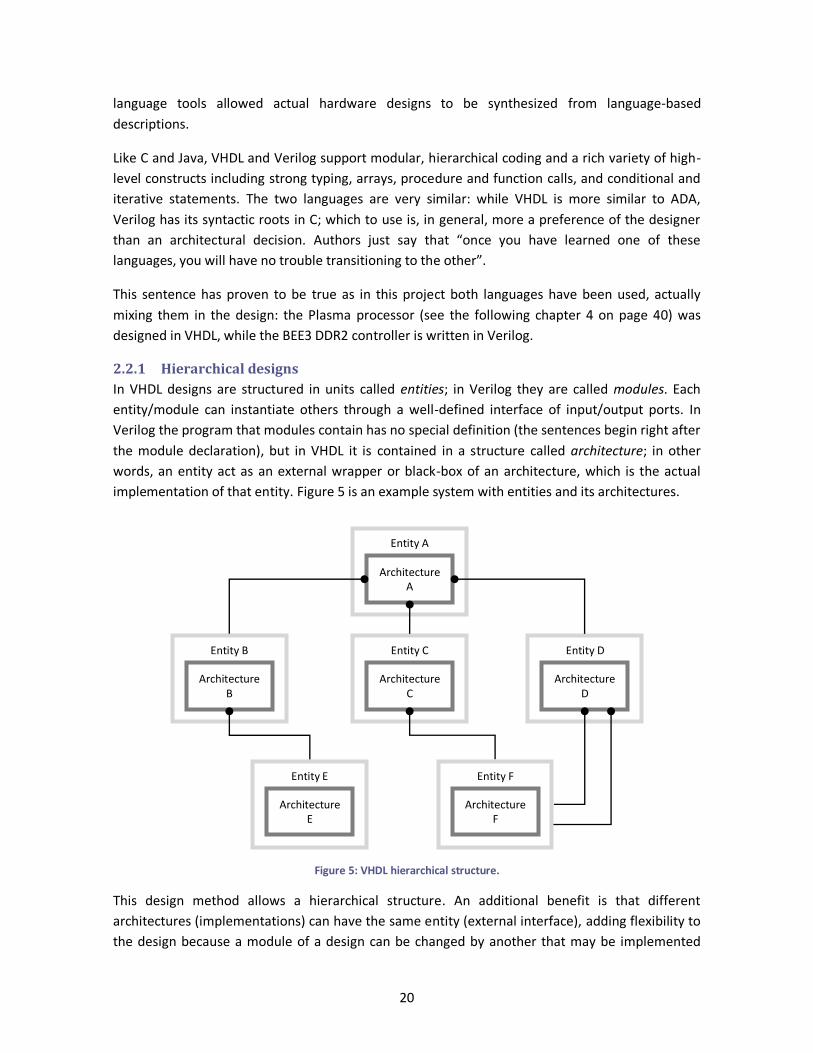
In VHDL designs are structured in units called entities; in Verilog they are called modules. Each
entity/module can instantiate others through a well-defined interface of input/output ports. In
Verilog the program that modules contain has no special definition (the sentences begin right after
the module declaration), but in VHDL it is contained in a structure called architecture; in other
words, an entity act as an external wrapper or black-box of an architecture, which is the actual
implementation of that entity. Figure 5 is an example system with entities and its architectures.
Figure 5: VHDL hierarchical structure.
This design method allows a hierarchical structure. An additional benefit is that different
architectures (implementations) can have the same entity (external interface), adding flexibility to
the design because a module of a design can be changed by another that may be implemented
Entity A
Architecture A
Entity B
Architecture B
Entity C
Architecture C
Entity D
Architecture D
Entity E
Architecture E
Entity F
Architecture F
21
differently without having to modify any parts of the system using it; in this sense, modules and
entities are similar to classes in object-oriented programming.
In the following sections, the design blocks will be called indistinctively modules or entities when
describing concepts applicable to both VHDL and Verilog.
2.2.2 Wires, signals and registers
Entities define their external interface with input and output ports of a given size (ports wider than
1 bit are called buses). Internal connections are called wires or signals, and interconnect external
ports and logic elements like other entities. In Verilog there are two kinds of connections: wires,
which act like a logical connection, and registers, which usually are used as flip-flops that can hold
their value. In VHDL not exists this distinction and both are called signals, but in the end it is the
compiler who decides whether to consider a wire, register or signal as a pure connection or a
memory register.
These are the basic building elements that combined with logical operators and language
constructs define a digital design. Usually signals, registers and wires represent a logical bit or a
given amount of logical bits (a bus or a multi-bit register), but different types can be specified. For
example, a signal can be of type integer, or even an array of 32-bit values that will likely be
translated to a multiplexor.
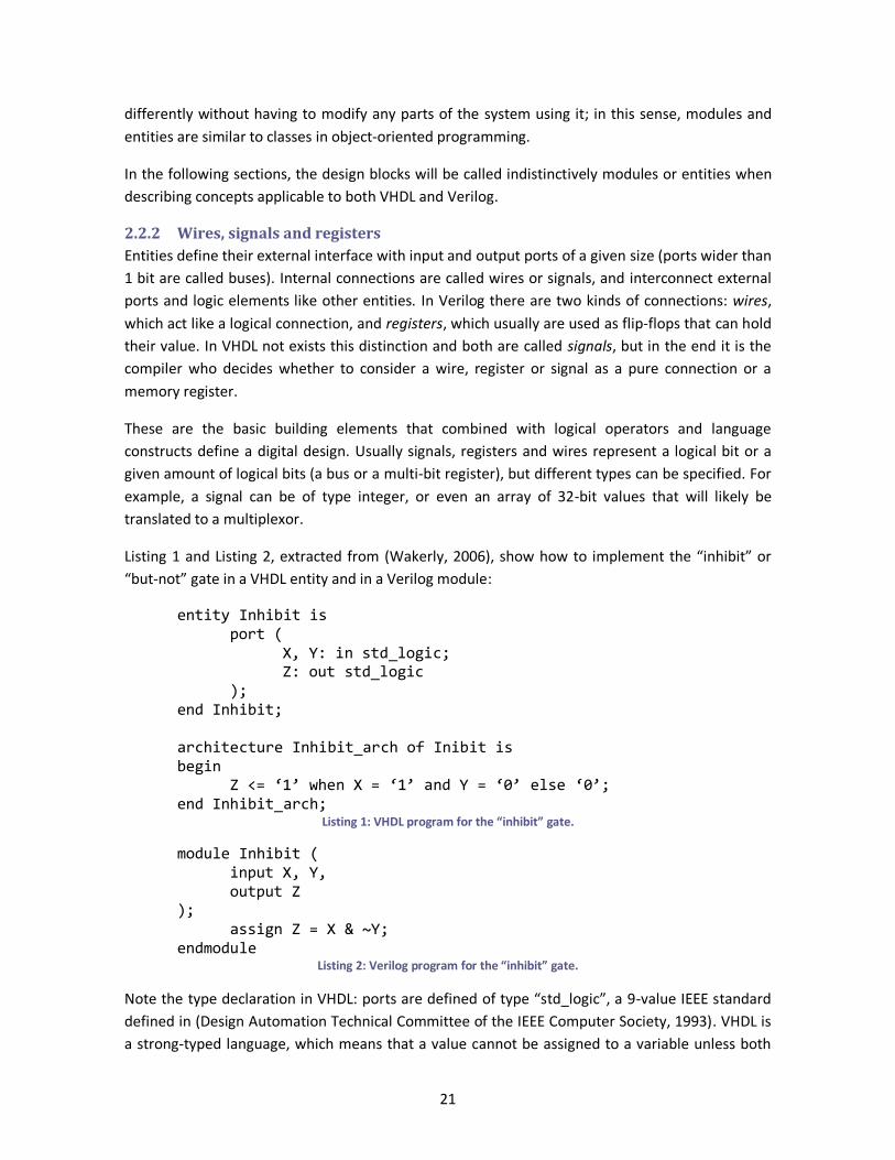
Listing 1 and Listing 2, extracted from (Wakerly, 2006), show how to implement the “inhibit” or
“but-not” gate in a VHDL entity and in a Verilog module:
entity Inhibit is port (
X, Y: in std_logic; Z: out std_logic
); end Inhibit; architecture Inhibit_arch of Inibit is begin
Z <= ‘1’ when X = ‘1’ and Y = ‘0’ else ‘0’; end Inhibit_arch;
Listing 1: VHDL program for the “inhibit” gate.
module Inhibit ( input X, Y, output Z
); assign Z = X & ~Y;
endmodule Listing 2: Verilog program for the “inhibit” gate.
Note the type declaration in VHDL: ports are defined of type “std_logic”, a 9-value IEEE standard
defined in (Design Automation Technical Committee of the IEEE Computer Society, 1993). VHDL is
a strong-typed language, which means that a value cannot be assigned to a variable unless both
22
have exactly the same type. Verilog is much more flexible in its types and its constructs, and
programs tend to be less formal than in VHDL, just like C is more flexible and has more coding
tricks than Java.
2.2.3 Behavioral vs. structural elements
Programs written in HDL are different than traditional sequential programs. Instructions do not
execute sequentially, but they are executed concurrently1, because the design is expanded
spatially among the circuitry and each instruction is mapped to an actual hardware resource that
will run independently from resources. These design constructs are called structural elements.
Structural elements are the top-level instructions of an HDL program, and can be a simple logic
gates construct that performs a logic equation (like the previous examples in Listing 1 and Listing
2). But as it executes the operations in parallel to other surrounding elements, it’s obvious that its
internal behavior is not parallel or concurrent, it is sequential: the designer expects the logic
formula to be performed in a given order, maintaining the operator’s priority. Thus, structural
elements can be made of behavioral elements that can be expected to be executed in a given
order.
For example, a state machine is a behavioral element as it performs different operations
depending on the internal state, and usually depends on a digital clock to change this state.
Another example can be a simple flip-flop or a RAM memory, which also has to wait for a clock
before reading or writing values.
VHDL’s key behavioral element is the process, which is a collection of sequential statements and
can include one or more variables, which are slightly different than signals and its scope is only the
process. Each process has a sensitivity list that specifies what signals its execution depends on;
every time one of these signals change, the process is executed completely. In Verilog behavioral
constructs are specified inside always clauses, which also include a sensitivity list.
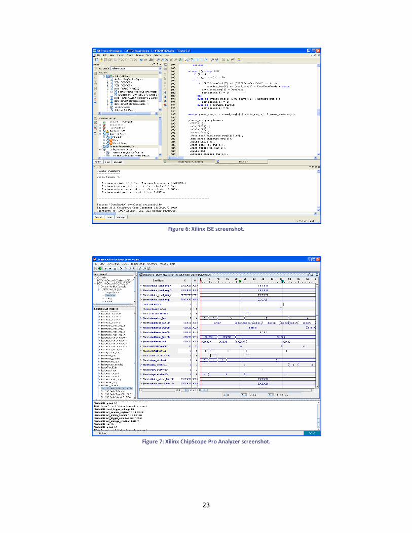
2.3 FPGA CAD tools Nowadays the hardware development is entirely done with the help of computer software.
Computer aided design (CAD) provides tools for each step of the hardware circuits development
process, from designing to implementation and simulation.
Major FPGA manufacturers offer complete software suites specially designed for their products.
This project has been implemented on Xilinx FPGAs like the Spartan-3E starter kit and the Virtex 5
chips used by the BEE3 platform. The tools provided by Xilinx can be used together through a
graphical interface called ISE. Figure 6 shows the main window of the ISE Project Navigator.
1 This doesn’t mean that the results of each circuit can be obtained concurrently. Although each behavioral
part can be executed independently of the others, usually they depend on each other and at the end the iterative behavior of the whole system can be similar to a sequential one.
23
Figure 6: Xilinx ISE screenshot.
Figure 7: Xilinx ChipScope Pro Analyzer screenshot.
24
The ISE Project Navigator organizes the project’s files and gives direct access to all the tools of the
software suite. The design can include source code written in VHDL or Verilog, Xilinx NGC
hardware circuits, schematic designs and many other formats, along with configuration files for
chip’s external pins, timing constraints and memory locations. The XST program (Xilinx Synthesizer
Tool) compiles the sources into a logic gates design, and other tools route and place the logic into
concrete logic slices.
The user can leave the implementation to the software, or make use of some tools that can edit
the design in every stage. And the circuits can be simulated on the computer or monitored directly
from the FPGA. This last option is possible thanks to the Xilinx ChipScope Pro software, which
inserts a special core in the design that stores the value of selected wires. The information can be
downloaded and displayed with the ChipScope Analyzer as a waveform. A screenshot can be seen
in Figure 7.
This explains why FPGAs are a great help for hardware developers: they offer a clean view of the
circuits in every stage of the development process.
2.4 The Berkeley Emulator Engine version 3 Multi-FPGA platforms are well-known devices. We can find such systems in the late 1980, and they
have evolved in different ways from small reconfigurable coprocessors attached to a computer to
big supercomputing systems (Hauck, et al., 2008). The BEE3 platform is the last member of an old
and big family.
Although this project started with a small Xilinx Spartan-3E FPGA board, mainly because the target
processor was designed over this platform, one of the main goals was to move the system to a
bigger, cutting-edge FPGA platform that would allow a realistic, intensive multiprocessor
emulation. The BEE3 platform largely fulfills these characteristics.
2.4.1 Previous multi-FPGA systems
There are a lot of systems that make use of the FPGA technology, but only a few that can be
considered to be built form FPGA or FPGA-like devices. In the late 1980 three multi-FPGA systems
were built, having in common that all communicated to a host computer across a standard system
bus in a traditional processor/coprocessor arrangement, and their primary goal was reconfigurable
computing.
The Programmable Active Memories (PAM) project started by Digital Equipment Corporation
(DEC) included four Xilinx XC3000-series FPGAs. The PAM Perle-0 board contained 25 Xilinx
XC3090 FPGAs in a 5 × 5 array, with four 64 KB RAM banks. It soon was upgraded to the newer
XC4000 series. Later designs could be plugged to a standard PCI bus in a PC or workstation, and
commercial versions became popular as research platforms. The Virtual Computer from the Virtual
Computer Corporation (VCC) was perhaps the first commercially available platform, and it was
slightly different from PAM. The first version arranged Xilinx XC4010 devices and I-Cube
programmable interconnect devices in a checkerboard pattern. And finally, the Splash system built
for the U.S. Department of Defense was maybe the most used of these systems. The Splash 2
25
board consisted of two rows of Xilinx XC4010 devices each with a small local memory. These 16
FPGA/memory pairs were connected to a crossbar switch controlled by another FPGA/memory
pair.
But PAM, VCC and Splash were relatively large systems. Around 1990 FPGA devices had an
expensive cost, so small systems were developed too. For example, the PRISM coprocessor, which
used a single small FPGA as a coprocessor in a large, distributed system. Or the Configurable Array
Logic (CAL), a small FPGA that could reconfigure logic cells each one individually. Later the
company that designed CAL, Algotronix, was acquired by Xilinx, who developed a second-
generation CAL, called XC6200.
A frequent requirement in those years was the circuit emulation. Digital circuitry simulation
became the bottleneck of the design process, and as the processors became large and complex,
FPGA emulators were increasingly valuable to designers. One of the first notable FPGA-based
hardware emulator was the Rapid Prototyping engine for Multiprocessors (RPM), which was
designed to prototype multiple-instruction multiple-data (MIMD) memory systems (Engels, et al.,
1991). RPM had an array of SPARC processors communicating with FPGA devices via an
interconnection bus. Thus the cache and memory controller circuits could be modeled and
emulated, helping the test of different multiprocessor memory systems on a fixed hardware
platform.
On 2005 the Flexible Architecture for Simulation and Testing (FAST) was developed to test thread
level parallelism (TLP) architectures (Davis, et al., 2005). Like RPM, it had a fixed processor and
configurable memory and I/O subsystems: it had 4 tiles each with a MIPS R3000 processor, 1 MB
of RAM memory and two FPGAs to model the cache and the coherency circuit. Two additional
FPGAs provided the processor interconnection bus and its controller.
As shown in the rest of this chapter, even the most modern, FPGA-based emulation systems can
be barely compared to the BEE platforms in terms of amount of resources provided, device speed
or flexibility.
2.4.2 Previous BEE versions
In 2001 the Berkeley Wireless Research Center (BWRC) of the University of California started the
design of a huge FPGA-based system, the Berkeley Emulation Engine (BEE) (Chang, et al., 2003).
The primary goal was to develop a digital signal processing engine with four objectives in mind:
reconfiguration, high performance, rapid prototyping and low-power consumption. The first use
was related to wireless communications research.
The BEE system had 20 Xilinx Virtex-E FPGAs and an I/O bandwidth of 200 gigabits per second. The
authors claim that the system, running at 60 MHz, had an equivalent capacity of 10 million ASIC
gates and a verified output of 600,000 millions 16-bit additions per second.
26
Figure 8: BEE system. Figure 9: BEE interconnection network.
A few years later (2005) the second version was presented (Chang, et al., 2005). The BEE2, defined
as a high-end reconfigurable computer (HERC), was designed to help computationally intensive
problems that involve high-performance computing and supercomputing. As the first version, it
was highly customizable and efficient (measured in throughput per unit cost and power
consumption).
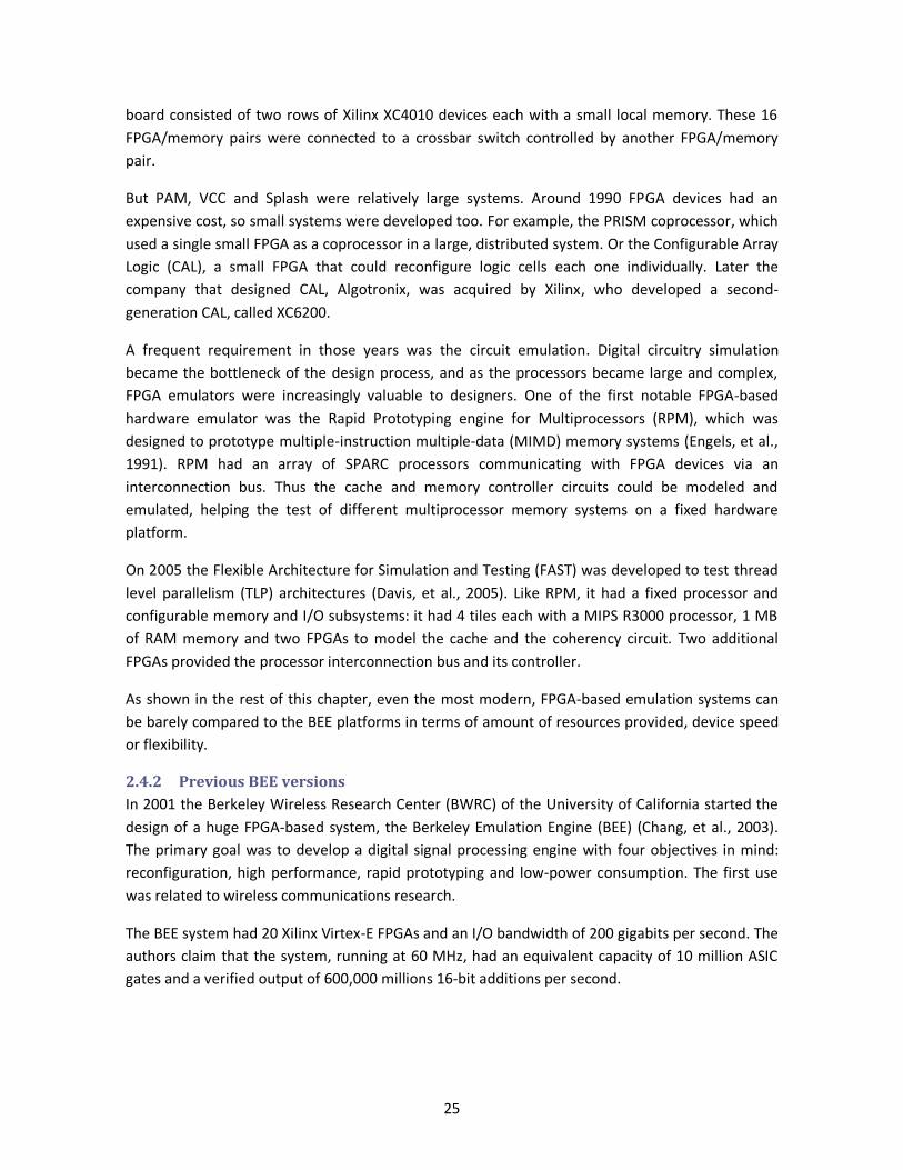
Figure 10: BEE2 system. Figure 11: BEE2 architecture.
The main difference with its predecessor was the topology. The first BEE had a mesh topology with
20 FPGAs connected through crossbars (XBAR). In contrast, the second version had 4 high-density
FPGAs (plus an additional fifth control FPGA) connected through a bidirectional ring bus. This last
topology remained until the last version, the BEE3.
2.4.3 BEE version 3
On 2007 the BEE project was consolidated and a number of companies and universities supported
it. While the academia focused on the RAMP research project, industry (especially Microsoft and
Xilinx) developed the third version of the FPGA platform. Microsoft, aided by some of the RAMP
members, designed and implemented the system and licensed it to a new company called
BEECube.
As explained in the title of the report “BEE3: Revitalizing Computer Architecture Research” (Davis,
et al., 2009), the main objective of the BEE3 was quite different than the objective of the initial
27
BEE system: from a system that could emulate rapidly prototyped designs, this new version was
focused to computer architecture research, in special hardware design testing and multiprocessor
research.
The BEE3 architecture is similar to its previous version, but the overall complexity has been
reduced and it doesn’t require an additional control FPGA. It has four state-of-the-art Xilinx Virtex
5 FPGAs2 with several improvements compared to the Virtex 2 devices of BEE2 and the previous
Virtex 4. They provide six-input lookup tables, which improves logic density over the earlier four-
input LUTs. They also have larger Block RAMs, and better I/O pin design, which improves signal
integrity. The LUTs may also be employed as 64 × 1 memories. The LX155T parts used in BEE3
contain 97,280 LUT-flipflop pairs, 212 36K-bit Block RAMs, and 128 DSP slices.
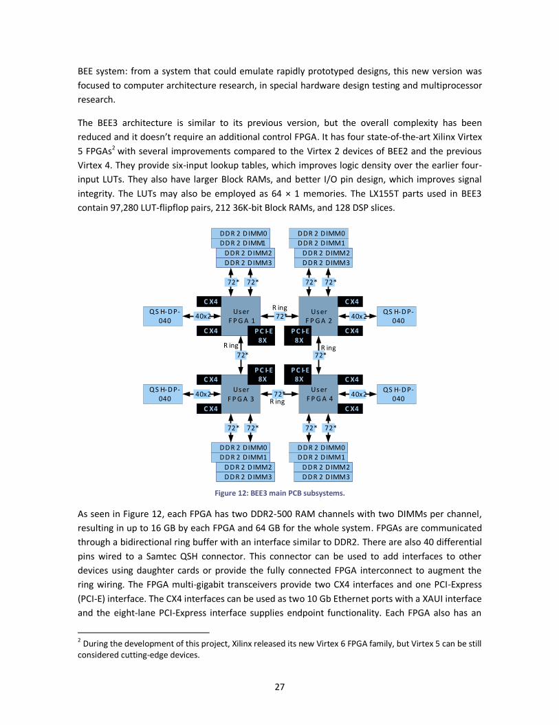
Figure 12: BEE3 main PCB subsystems.
As seen in Figure 12, each FPGA has two DDR2-500 RAM channels with two DIMMs per channel,
resulting in up to 16 GB by each FPGA and 64 GB for the whole system. FPGAs are communicated
through a bidirectional ring buffer with an interface similar to DDR2. There are also 40 differential
pins wired to a Samtec QSH connector. This connector can be used to add interfaces to other
devices using daughter cards or provide the fully connected FPGA interconnect to augment the
ring wiring. The FPGA multi-gigabit transceivers provide two CX4 interfaces and one PCI-Express
(PCI-E) interface. The CX4 interfaces can be used as two 10 Gb Ethernet ports with a XAUI interface
and the eight-lane PCI-Express interface supplies endpoint functionality. Each FPGA also has an
2 During the development of this project, Xilinx released its new Virtex 6 FPGA family, but Virtex 5 can be still considered cutting-edge devices.
28
embedded 1 Gb Ethernet (GbE) MAC hard macro that is coupled to a Broadcom PHY chip. The
other major components on the BEE3 PCB are the real-time clock (RTC) and EEPROM that can be
used by an OS and to store MAC addresses and other FPGA-specific information. In addition, there
are several user-controlled LEDs and a global and an FPGA-specific reset button located on the
BEE3 PCB and on the enclosure front panel.
The board is packaged in a 2U rack-mountable enclosure that helps the development of scalable
systems. For example, the RAMP Blue project provides up to 1008 processors using 21 BEE2
boards on a 42U rack (Burke, et al., 2008).
2.4.4 The BEE3 DDR2 controller
Due to its high cost, it is obvious that this emulation platform won’t replace the software
simulators (Davis, et al., 2009). To guarantee the continuity of research projects like RAMP and
attract the interest of other researchers and companies to the BEE3 platform, a minimal
development software stack and had to be available from FPGA designs, or “gateware”, to
traditional software to run on them, like operative systems and software libraries.
The objective was to create a community that shared research and designs, all of them based on
the same hardware platform. One of the first blocks of this building is the DDR2 memory controller
(Thacker, 2009) that gives access to the complex BEE3 memory system, freely available from
Microsoft Research.
As explained before, the BEE3 system contains four Virtex-5 FPGAs. Each FPGA controls four DDR2
DIMMs, organized as two independent 2-DIMM memory channels. The DDR2 controller available
from Microsoft manages one of those channels. The design is written in the Verilog HDL language,
and contains two DDR2 modules to control the two ranks of the DIMM, and two instances of a
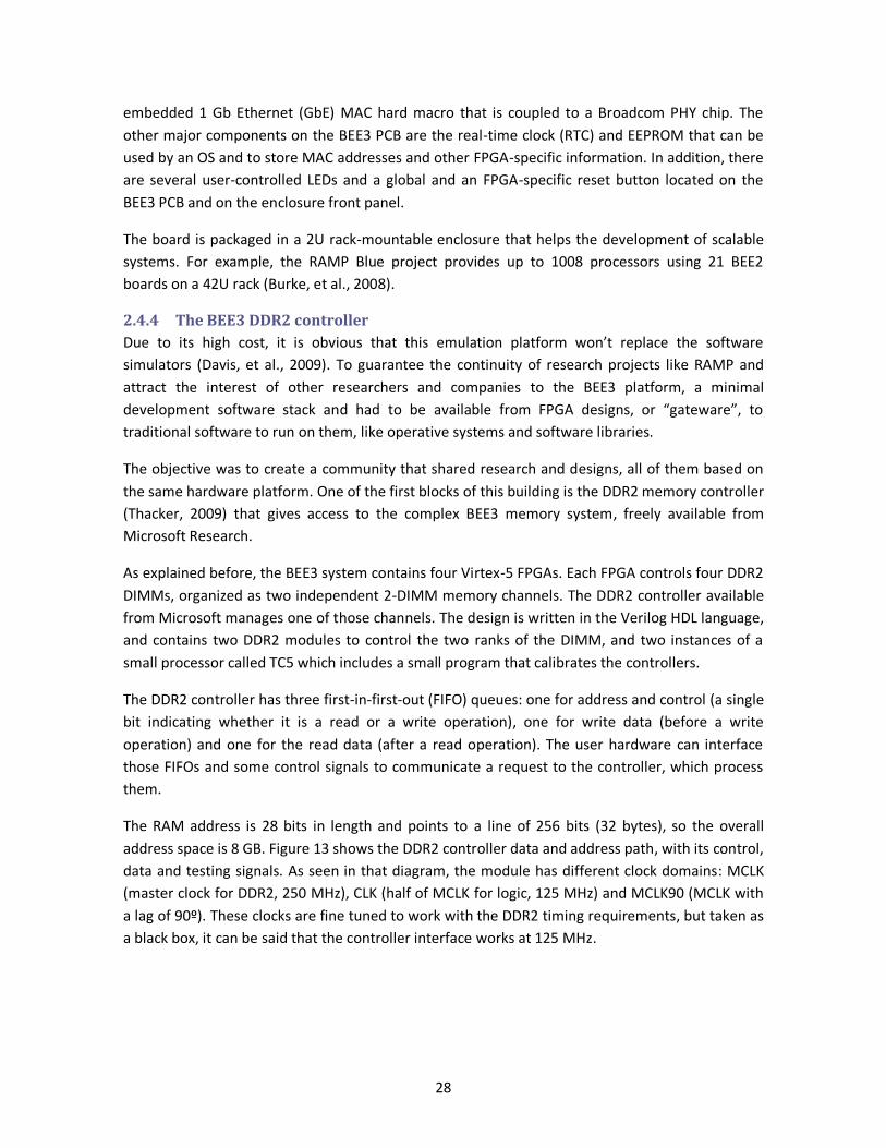
small processor called TC5 which includes a small program that calibrates the controllers.
The DDR2 controller has three first-in-first-out (FIFO) queues: one for address and control (a single
bit indicating whether it is a read or a write operation), one for write data (before a write
operation) and one for the read data (after a read operation). The user hardware can interface
those FIFOs and some control signals to communicate a request to the controller, which process
them.
The RAM address is 28 bits in length and points to a line of 256 bits (32 bytes), so the overall
address space is 8 GB. Figure 13 shows the DDR2 controller data and address path, with its control,
data and testing signals. As seen in that diagram, the module has different clock domains: MCLK
(master clock for DDR2, 250 MHz), CLK (half of MCLK for logic, 125 MHz) and MCLK90 (MCLK with
a lag of 90º). These clocks are fine tuned to work with the DDR2 timing requirements, but taken as
a black box, it can be said that the controller interface works at 125 MHz.
29
Figure 13: BEE3 DDR controller data and address paths.
The inherent complexity of the DDR2 protocol needs some calibration to assure the correctness of
data communications. Hardcoding the operations and DDR2 signaling would be highly complex as
it is difficult to program certain timings and delays in a hardware-based state machine, and such
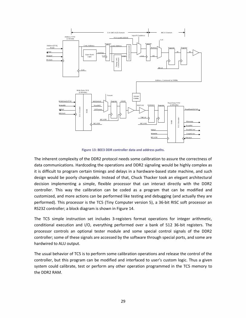
design would be poorly changeable. Instead of that, Chuck Thacker took an elegant architectural
decision implementing a simple, flexible processor that can interact directly with the DDR2
controller. This way the calibration can be coded as a program that can be modified and
customized, and more actions can be performed like testing and debugging (and actually they are
performed). This processor is the TC5 (Tiny Computer version 5), a 36-bit RISC soft processor an
RS232 controller; a block diagram is shown in Figure 14.
The TC5 simple instruction set includes 3-registers format operations for integer arithmetic,
conditional execution and I/O, everything performed over a bank of 512 36-bit registers. The
processor controls an optional tester module and some special control signals of the DDR2
controller; some of these signals are accessed by the software through special ports, and some are
hardwired to ALU output.
The usual behavior of TC5 is to perform some calibration operations and release the control of the
controller, but this program can be modified and interfaced to user’s custom logic. Thus a given
system could calibrate, test or perform any other operation programmed in the TC5 memory to
the DDR2 RAM.
30
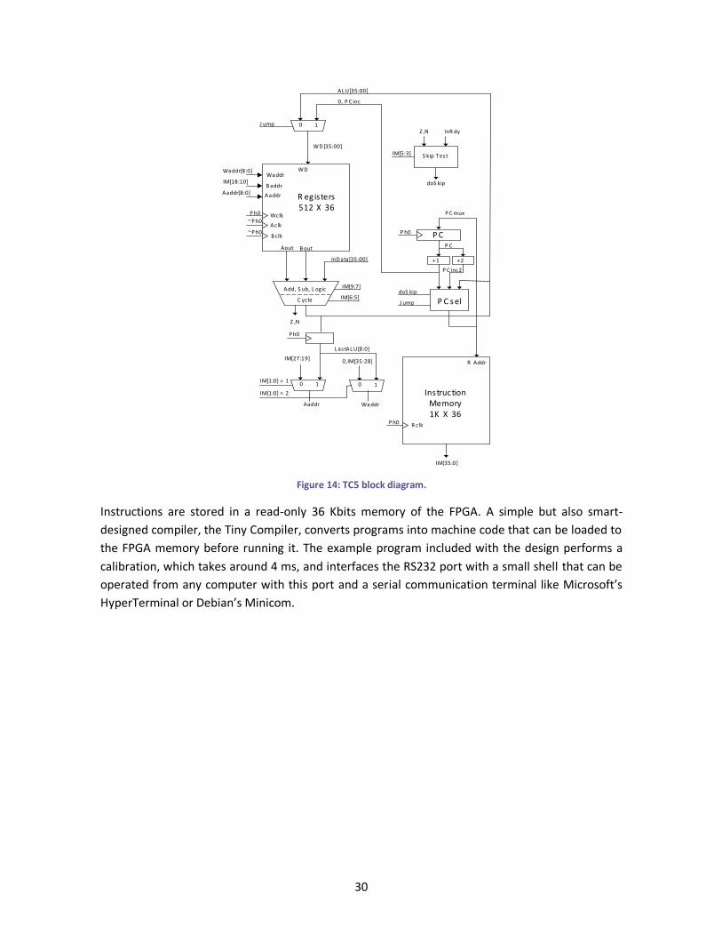
Figure 14: TC5 block diagram.
Instructions are stored in a read-only 36 Kbits memory of the FPGA. A simple but also smart-
designed compiler, the Tiny Compiler, converts programs into machine code that can be loaded to
the FPGA memory before running it. The example program included with the design performs a
calibration, which takes around 4 ms, and interfaces the RS232 port with a small shell that can be
operated from any computer with this port and a serial communication terminal like Microsoft’s
HyperTerminal or Debian’s Minicom.
31
3 MIPS and the RISC architectures
Historically, the evolution of computer architectures has been dominated by families of
increasingly complex processors. Under market pressures, complex instruction set computer (CISC)
architectures introduced more and more new instructions that added specific features, like high-
level languages or operating system support, or just aggregated simple operations to save space
and sometimes time.
The prevalence of high-level languages, the development of compilers that can optimize at the
microcode level and the advances in memory and bus speeds favored, however, that a new
conception of processor architecture had appeared to focus on some problems of the CISC
architecture. The Reduced Instruction Set Computer (RISC) architecture’s key ideas go beyond
reducing or simplifying the instruction set, which is more a side effect, and the whole conception
emerges from the analysis of the “real” needs of applications, and if compilers actually make use
of the operations provided by the processor. Perhaps the best definition can be found in (Kane, et
al., 1992):
RISC concepts emerged from a statistical analysis of how software actually
uses the resources of the processor.
Although the RISC architectures are not as popular as the CISC are, especially in the case of Intel’s
x86 architecture and its descendants, vast markets have emerged in the field of embedded
systems like mobile phones and portable computers. MIPS, SPARC, ARM and PowerPC 3
architectures are becoming popular for their simplicity, small size and low power consume.
3.1 MIPS, the RISC pioneers In 1981 a team from the Stanford University leaded by John L. Hennessy started to work with the
principles of the RISC architecture, like pipelining and reducing and simplifying the instruction set.
Soon the researchers found great benefits, such as the possibility of increasing the processor’s
clock and reducing the size of the chips, along with other side benefits, like a uniform ISA and a
3 Although PowerPC was known by being the processor used in Apple’s computers, it is still widely used. It
can be found in the new Cell multicore architecture, developed by Sony, Toshiba and IBM, which makes use of a similar ISA, and is manufactured in ASIC designs sold by IBM.
32
shorter design cycle. In 1984 some of the researchers created a company to exploit commercially
their new design, the Microprocessor without Interlocked Pipeline Stages (MIPS).
The first MIPS designs, the R-series, are 32-bit processors with no significant architectural
variations, but some interesting implementation modifications. For example, the R4000 processor
introduces the dual-page translation lookaside buffer (TLB) entries, and R6000 integrates its TLB in
the secondary cache. After a few new years, MIPS standardized their architectures in two
specifications: MIPS 32 and MIPS 64.
This work focuses on the R3000 and R4000 designs and their instructions set MIPS I.
In the following sections some of the MIPS RISC architectural principles are briefly discussed. Most
of the information has been extracted from (Kane, et al., 1992), edited by MIPS Technologies, Inc.
It covers in an exhaustive way the MIPS R2000 and R3000 architectures, with dozens of technical
details about hardware implementation (which in MIPS designs is carefully separated from
specification). This book is also interesting because it helps to understand why the designers took
such architectural decisions in the decade of ’80. Actually the MIPS architecture was very new at
the time this book was written and the designs introduced have had many changes.
3.1.1 Efficient pipelining
When the Stanford team was researching the RISC architecture, pipelining was a well known
technique, and obviously nowadays it is not an exclusive part of the RISC domain. But it hadn’t
been developed into its full potential (Sweetman, 2007).
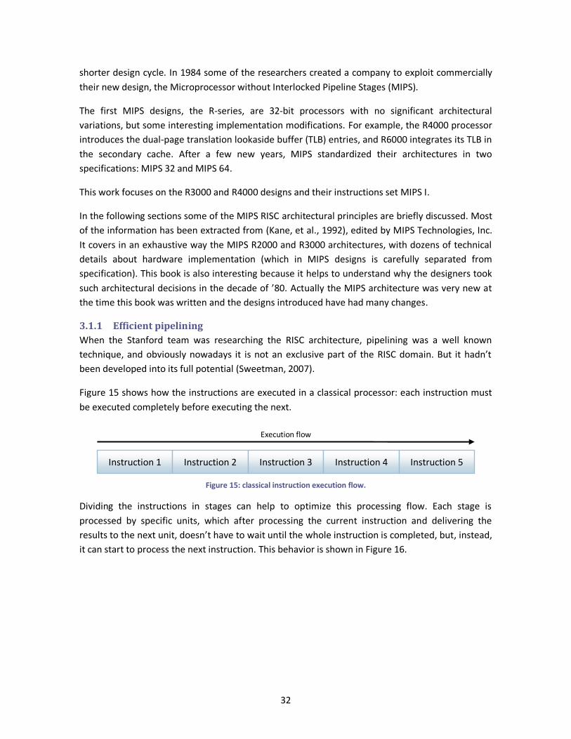
Figure 15 shows how the instructions are executed in a classical processor: each instruction must
be executed completely before executing the next.
Figure 15: classical instruction execution flow.
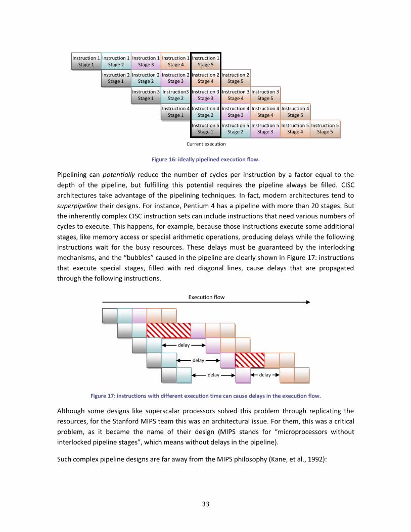
Dividing the instructions in stages can help to optimize this processing flow. Each stage is
processed by specific units, which after processing the current instruction and delivering the
results to the next unit, doesn’t have to wait until the whole instruction is completed, but, instead,
it can start to process the next instruction. This behavior is shown in Figure 16.
Instruction 1 Instruction 2 Instruction 3 Instruction 4 Instruction 5
Execution flow
33
Figure 16: ideally pipelined execution flow.
Pipelining can potentially reduce the number of cycles per instruction by a factor equal to the
depth of the pipeline, but fulfilling this potential requires the pipeline always be filled. CISC
architectures take advantage of the pipelining techniques. In fact, modern architectures tend to
superpipeline their designs. For instance, Pentium 4 has a pipeline with more than 20 stages. But
the inherently complex CISC instruction sets can include instructions that need various numbers of
cycles to execute. This happens, for example, because those instructions execute some additional
stages, like memory access or special arithmetic operations, producing delays while the following
instructions wait for the busy resources. These delays must be guaranteed by the interlocking
mechanisms, and the “bubbles” caused in the pipeline are clearly shown in Figure 17: instructions
that execute special stages, filled with red diagonal lines, cause delays that are propagated
through the following instructions.
Figure 17: instructions with different execution time can cause delays in the execution flow.
Although some designs like superscalar processors solved this problem through replicating the
resources, for the Stanford MIPS team this was an architectural issue. For them, this was a critical
problem, as it became the name of their design (MIPS stands for “microprocessors without
interlocked pipeline stages”, which means without delays in the pipeline).
Such complex pipeline designs are far away from the MIPS philosophy (Kane, et al., 1992):
delay
delay
delay delay
Execution flow
Instruction 1 Stage 1
Instruction 1 Stage 2
Instruction 1 Stage 3
Instruction 1 Stage 4
Instruction 1 Stage 5
Instruction 2 Stage 1
Instruction 2 Stage 2
Instruction 2 Stage 3
Instruction 2 Stage 4
Instruction 2 Stage 5
Instruction 3 Stage 1
Instruction3 Stage 2
Instruction 3 Stage 3
Instruction 3 Stage 4
Instruction 3 Stage 5
Instruction 4 Stage 1
Instruction 4 Stage 2
Instruction 4 Stage 3
Instruction 4 Stage 4
Instruction 4 Stage 5
Instruction 5 Stage 1
Instruction 5 Stage 2
Instruction 5 Stage 3
Instruction 5 Stage 4
Instruction 5 Stage 5
Current execution
34
A primary goal of RISC designs is to define an instruction set where
execution of most, if not all, instructions requires a uniform number of
cycles and, ideally, achieves a minimum execution rate for each clock cycle.
3.1.2 A reduced and simple instruction set
The rule followed by the MIPS team while designing their instruction set was to add a new
instruction if, and only if, there was a significant performance improvement. Specifically, there
should be at least a verifiable 1% performance gain over a range of applications (Kane, et al., 1992;
Mashley, 1989).
A reduced and simple instruction set is necessary to avoid instructions with variable execution
time, and to allow a high clock rate. As in other RISC architectures, this causes an increase in the
number of instructions per task, and can be argued that in RISC architectures more instructions
are necessary than in a CISC architecture. MIPS designers tried to solve this problem at software
level with an intense compilation optimization.
This is possible thanks to the reduced instruction set and some MIPS special features, like load and
branch slots: in a MIPS processor, the next instruction after jump (the branch slot) is always
executed no matter the evaluation of the branch condition, and the result of a load instruction is
only available after one instruction (the load slot). In the code shown in Listing 3, the instruction 4
cannot obtain the value loaded by the instruction 2 immediately, so the no-operation instruction 3
must be inserted as a delay.
1: load r1, A 2: load r2, B 3: nop ← load delay slot 4: add r3, r1, r2
Listing 3: load delay slot.
Another typical CISC feature, the operating system dedicated instructions, are not usually included
in the MIPS architectures because the designers observed that compilers rarely use it. Following
the simplicity rule, system management tasks are managed by software, if possible with
combinations of simple instructions. This can be observed in the input/output interface (it is
mapped to memory, so there isn’t an x86 in/out instructions equivalent) or the interruption
returning mechanism used in the primitive designs (a special instruction to enable interruptions
inserted in a branch delay slot).
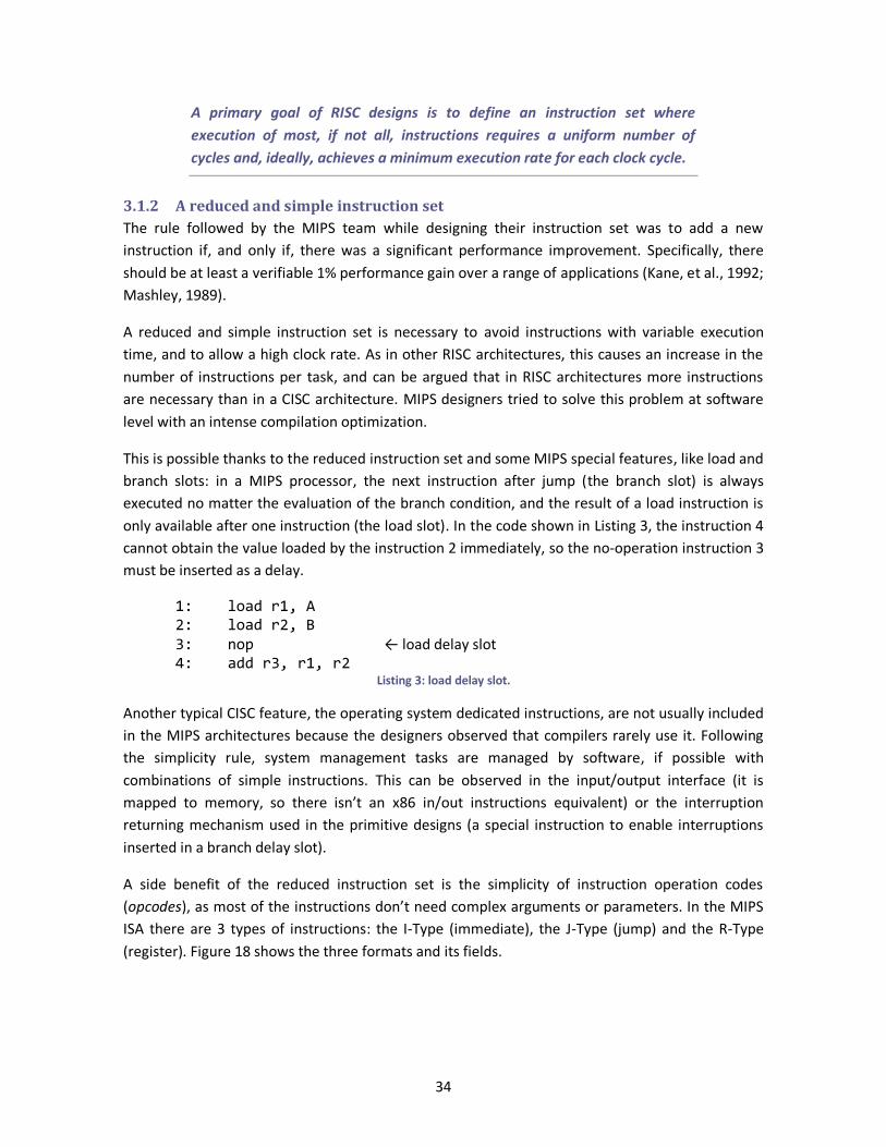
A side benefit of the reduced instruction set is the simplicity of instruction operation codes
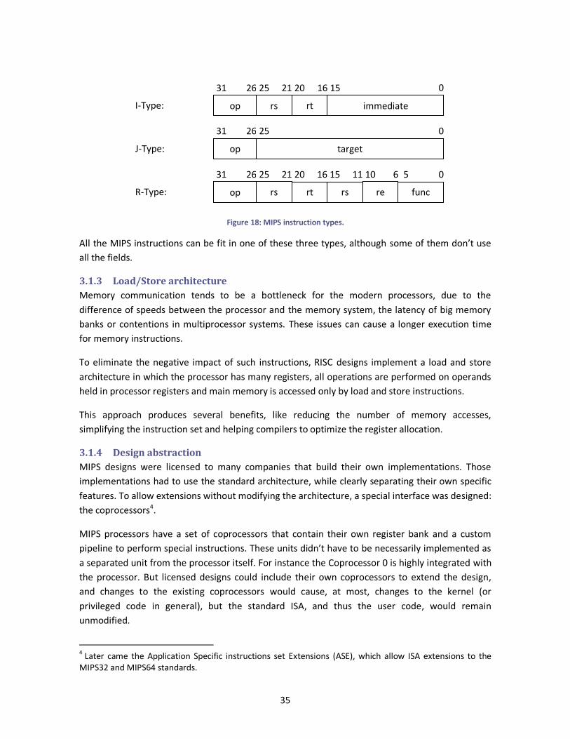
(opcodes), as most of the instructions don’t need complex arguments or parameters. In the MIPS
ISA there are 3 types of instructions: the I-Type (immediate), the J-Type (jump) and the R-Type
(register). Figure 18 shows the three formats and its fields.
35
Figure 18: MIPS instruction types.
All the MIPS instructions can be fit in one of these three types, although some of them don’t use
all the fields.
3.1.3 Load/Store architecture
Memory communication tends to be a bottleneck for the modern processors, due to the
difference of speeds between the processor and the memory system, the latency of big memory
banks or contentions in multiprocessor systems. These issues can cause a longer execution time
for memory instructions.
To eliminate the negative impact of such instructions, RISC designs implement a load and store
architecture in which the processor has many registers, all operations are performed on operands
held in processor registers and main memory is accessed only by load and store instructions.
This approach produces several benefits, like reducing the number of memory accesses,
simplifying the instruction set and helping compilers to optimize the register allocation.
3.1.4 Design abstraction
MIPS designs were licensed to many companies that build their own implementations. Those
implementations had to use the standard architecture, while clearly separating their own specific
features. To allow extensions without modifying the architecture, a special interface was designed:
the coprocessors4.
MIPS processors have a set of coprocessors that contain their own register bank and a custom
pipeline to perform special instructions. These units didn’t have to be necessarily implemented as
a separated unit from the processor itself. For instance the Coprocessor 0 is highly integrated with
the processor. But licensed designs could include their own coprocessors to extend the design,
and changes to the existing coprocessors would cause, at most, changes to the kernel (or
privileged code in general), but the standard ISA, and thus the user code, would remain
unmodified.
4 Later came the Application Specific instructions set Extensions (ASE), which allow ISA extensions to the MIPS32 and MIPS64 standards.
op rs rt immediate
op target
op rs rt rs re func
I-Type:
J-Type:
R-Type:
31
31
31
25 20 15 0
0
0
26
26
26
21
21 25
25
15 20
16
16 10 11 5 6
36
The most well-known coprocessors are the Coprocessor 0 (System Coprocessor), which manages
the virtual memory and exception handling; and the Coprocessor 1 (Floating Point Coprocessor).
3.1.5 An architecture aware of the memory system
MIPS designers were pioneers in implementing some of the today’s well-known techniques,
especially in its memory systems. Separated caches for data and instructions; on-chip primary and
secondary caches; double-page, resizable TLB entries and other techniques are currently common
features that were introduced in the late ’80 and early ’90. This gives an idea of the high
integration between the processor and the memory system, thanks to the overall simplicity of the
architecture. This integration allows a high performance data communication over the computer.
The interesting MIPS memory model (addressing, paging and caching) is explained in the next
sections, while compared with the Plasma and Honeycomb models.
3.1.6 Limitations
Although the elegance of the RISC architecture, especially in the MIPS designs, there are a number
of limitations and constraints that can surprise x86 programmers.
32 general purpose 32-bit registers. This is not a limitation, but as in other architectures
has some constraints and conventions that limit their usage. The register 0 is read only
and its value is always zero. The register 31 is reserved for the return address when calling
subroutines. See “Appendix A: processor registers” and “Appendix B: instruction set” for
more information about the CPU registers’ usage and the Jump And Link (JAL) instruction.
No testing flags or condition codes. Comparisons for conditional execution must be explicit
and always are performed and stored on registers.
Single addressing mode. Loads and stores select the memory location with a base register
modified by a 16-bit signed displacement.
32-bit operations. While data can be load and stored with different lengths (1, 2 and 4
bytes), data on registers is always treated as data of full register length.
No unaligned memory accesses. There is some support for unaligned data access at word
level (32 bit), but half-words must be aligned.
No special stack support. There is one register reserved by convention to contain the stack
pointer, but there isn’t any special hardware support for stack operations like push and
pop.
Minimal interrupt and exception support. As said in (Sweetman, 2007), “It is hard to see
how the hardware could do less.” When handling an exception or interruption (both are
hardly distinguishable) the processor saves the returning address, modifies the machine
state just enough to let the operating system know what happened and disables
interruptions. Context switches, and execution state saving and restoring, are left to the
software.
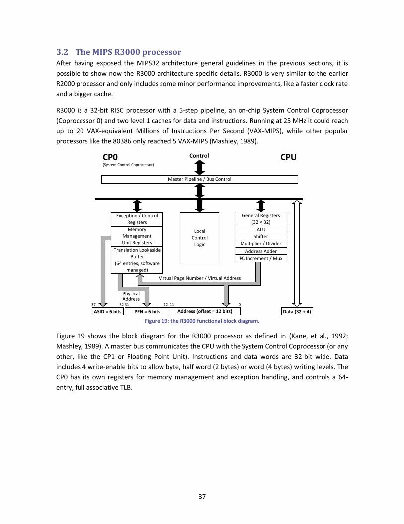
37
3.2 The MIPS R3000 processor After having exposed the MIPS32 architecture general guidelines in the previous sections, it is
possible to show now the R3000 architecture specific details. R3000 is very similar to the earlier
R2000 processor and only includes some minor performance improvements, like a faster clock rate
and a bigger cache.
R3000 is a 32-bit RISC processor with a 5-step pipeline, an on-chip System Control Coprocessor
(Coprocessor 0) and two level 1 caches for data and instructions. Running at 25 MHz it could reach
up to 20 VAX-equivalent Millions of Instructions Per Second (VAX-MIPS), while other popular
processors like the 80386 only reached 5 VAX-MIPS (Mashley, 1989).
Figure 19: the R3000 functional block diagram.
Figure 19 shows the block diagram for the R3000 processor as defined in (Kane, et al., 1992;
Mashley, 1989). A master bus communicates the CPU with the System Control Coprocessor (or any
other, like the CP1 or Floating Point Unit). Instructions and data words are 32-bit wide. Data
includes 4 write-enable bits to allow byte, half word (2 bytes) or word (4 bytes) writing levels. The
CP0 has its own registers for memory management and exception handling, and controls a 64-
entry, full associative TLB.
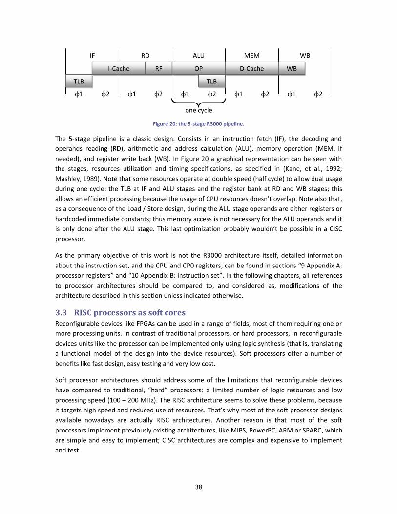
38
Figure 20: the 5-stage R3000 pipeline.
The 5-stage pipeline is a classic design. Consists in an instruction fetch (IF), the decoding and
operands reading (RD), arithmetic and address calculation (ALU), memory operation (MEM, if
needed), and register write back (WB). In Figure 20 a graphical representation can be seen with
the stages, resources utilization and timing specifications, as specified in (Kane, et al., 1992;
Mashley, 1989). Note that some resources operate at double speed (half cycle) to allow dual usage
during one cycle: the TLB at IF and ALU stages and the register bank at RD and WB stages; this
allows an efficient processing because the usage of CPU resources doesn’t overlap. Note also that,
as a consequence of the Load / Store design, during the ALU stage operands are either registers or
hardcoded immediate constants; thus memory access is not necessary for the ALU operands and it
is only done after the ALU stage. This last optimization probably wouldn’t be possible in a CISC
processor.
As the primary objective of this work is not the R3000 architecture itself, detailed information
about the instruction set, and the CPU and CP0 registers, can be found in sections “9 Appendix A:
processor registers” and “10 Appendix B: instruction set”. In the following chapters, all references
to processor architectures should be compared to, and considered as, modifications of the
architecture described in this section unless indicated otherwise.
3.3 RISC processors as soft cores Reconfigurable devices like FPGAs can be used in a range of fields, most of them requiring one or
more processing units. In contrast of traditional processors, or hard processors, in reconfigurable
devices units like the processor can be implemented only using logic synthesis (that is, translating
a functional model of the design into the device resources). Soft processors offer a number of
benefits like fast design, easy testing and very low cost.
Soft processor architectures should address some of the limitations that reconfigurable devices
have compared to traditional, “hard” processors: a limited number of logic resources and low
processing speed (100 – 200 MHz). The RISC architecture seems to solve these problems, because
it targets high speed and reduced use of resources. That’s why most of the soft processor designs
available nowadays are actually RISC architectures. Another reason is that most of the soft
processors implement previously existing architectures, like MIPS, PowerPC, ARM or SPARC, which
are simple and easy to implement; CISC architectures are complex and expensive to implement
and test.
IF RD ALU MEM WB
TLB
I-Cache RF OP D-Cache WB
TLB
φ1 φ2 φ1 φ2
φ1 φ2
φ1 φ2
φ1 φ2
one cycle

39
The same arguments can be applied to a chip multiprocessor when using several soft cores as
processing elements: RISC architectures are easily customizable and require few resources, so they
can be integrated into a big (more than 16 processors) multiprocessor chip.
40
4 Plasma, an open RISC processor
In previous chapters the MIPS R3000 processor has been introduced. This late 1980 RISC processor
executed the MIPS I instruction set at 25 MHz and included a System Control Coprocessor, or
known as Coprocessor 0, which provided virtual memory and exception handling. In this chapter a
MIPS R3000-compatible processor is exposed and compared to the original design.
As the general lines of the R3000 architecture have already been explained previously, only
significant architectural differences and outstanding implementation details will be referenced in
the next paragraphs.
4.1 Plasma CPU The Plasma CPU is a small synthesizable 32-bit RISC microprocessor designed by Steve Rhoads
(Rhoads, 2001). This soft processor is an open source implementation in VHDL of the MIPS R3000
processor released to the public domain on OpenCores, a repository of open hardware designs.
The architecture is organized in two levels: the CPU, which accomplishes the requirements for the
MIPS I instruction set, and other included subsystems; and the Plasma backplane that
interconnects the computer components and interfaces with the FPGA external ports.
The Plasma CPU has 9 modules; an overview of the interconnections can be seen in Figure 21. The
program counter unit controls what instruction will be loaded by the memory controller. When
loaded, the main controller converts the opcode into a 60-bit very long word instruction (VLWI)
that controls the rest of the modules: the register bank, the ALU with the integer shift and
multiplication units, and a central bus multiplexer. See chapters 9 (“Appendix A: processor
registers” on page 74) and 10 (“Appendix B: instruction set” on page 75) for a detailed
specification of what registers are available on the register bank, their usage, and how the
registers are coded into the instruction opcodes.
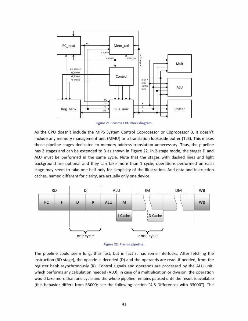
41
Figure 21: Plasma CPU block diagram.
As the CPU doesn’t include the MIPS System Control Coprocessor or Coprocessor 0, it doesn’t
include any memory management unit (MMU) or a translation lookaside buffer (TLB). This makes
those pipeline stages dedicated to memory address translation unnecessary. Thus, the pipeline
has 2 stages and can be extended to 3 as shown in Figure 22. In 2-stage mode, the stages D and
ALU must be performed in the same cycle. Note that the stages with dashed lines and light
background are optional and they can take more than 1 cycle; operations performed on each
stage may seem to take one half only for simplicity of the illustration. And data and instruction
caches, named different for clarity, are actually only one device.
Figure 22: Plasma pipeline.
The pipeline could seem long, thus fast, but in fact it has some interlocks. After fetching the
instruction (RD stage), the opcode is decoded (D) and the operands are read, if needed, from the
register bank asynchronously (R). Control signals and operands are processed by the ALU unit,
which performs any calculation needed (ALU); in case of a multiplication or division, the operation
would take more than one cycle and the whole pipeline remains paused until the result is available
(this behavior differs from R3000; see the following section “4.5 Differences with R3000”). The
PC_next Mem_ctrl
Control
Mult
ALU
ShifterBus_muxReg_bank
PC
d_write
rs_index
rt_index
rd_index
PC
rs
rt
rd
pc_source
opcode mem_src
a
b
c
mult /alu /shifterfunc
add
ress
_nex
t
RD
one cycle
D ALU IM WB
PC F ALU M D R WB
I Cache
DM
D Cache
≥ one cycle
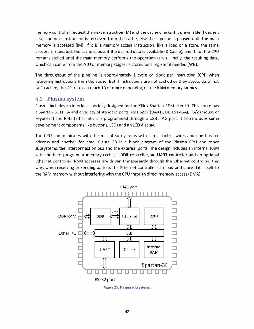
42
memory controller request the next instruction (M) and the cache checks if it is available (I Cache);
if so, the next instruction is retrieved from the cache, else the pipeline is paused until the main
memory is accessed (IM). If it is a memory access instruction, like a load or a store, the same
process is repeated: the cache checks if the desired data is available (D Cache), and if not the CPU
remains stalled until the main memory performs the operation (DM). Finally, the resulting data,
which can come from the ALU or memory stages, is stored on a register if needed (WB).
The throughput of the pipeline is approximately 1 cycle or clock per instruction (CPI) when
retrieving instructions from the cache. But if instructions are not cached or they access data that
isn’t cached, the CPI rate can reach 10 or more depending on the RAM memory latency.
4.2 Plasma system Plasma includes an interface specially designed for the Xilinx Spartan-3E starter kit. This board has
a Spartan-3E FPGA and a variety of standard ports like RS232 (UART), DE-15 (VGA), PS/2 (mouse or
keyboard) and RJ45 (Ethernet). It is programmed through a USB JTAG port. It also includes some
development components like buttons, LEDs and an LCD display.
The CPU communicates with the rest of subsystems with some control wires and one bus for
address and another for data. Figure 23 is a block diagram of the Plasma CPU and other
subsystems, the interconnection bus and the external ports. The design includes an internal RAM
with the boot program, a memory cache, a DDR controller, an UART controller and an optional
Ethernet controller. RAM accesses are driven transparently through the Ethernet controller; this
way, when receiving or sending packets the Ethernet controller can load and store data itself to
the RAM memory without interfering with the CPU through direct memory access (DMA).
Figure 23: Plasma subsystems.
CPU
UART Cache Internal
RAM
Ethernet
Bus
DDR DMA
DDR RAM
Other I/O
RS232 port
RJ45 port
Spartan-3E
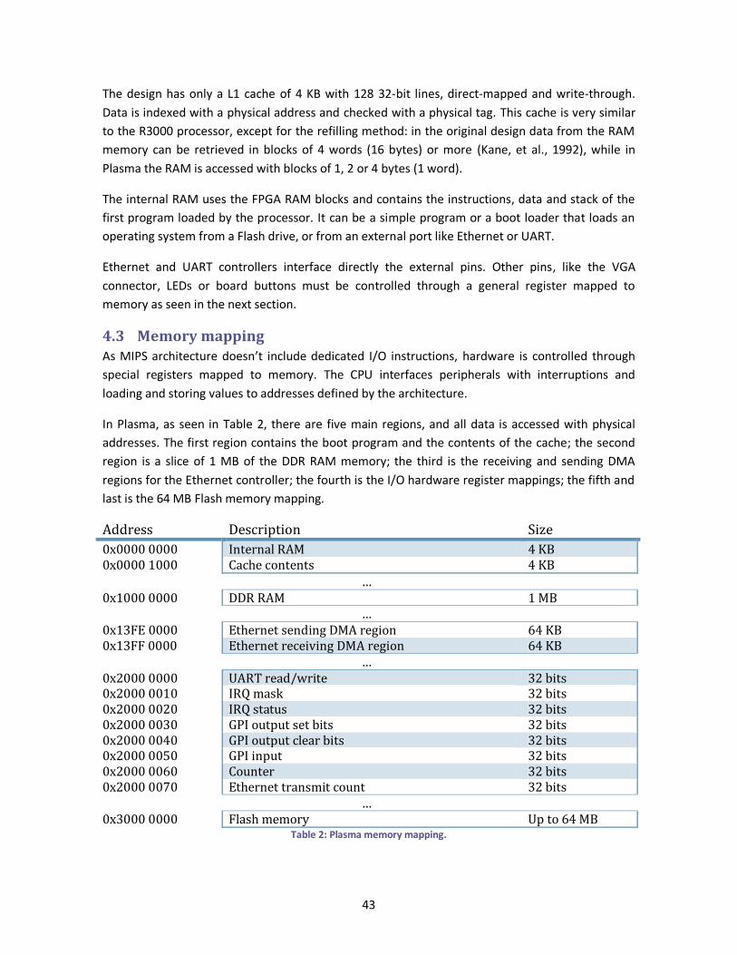
43
The design has only a L1 cache of 4 KB with 128 32-bit lines, direct-mapped and write-through.
Data is indexed with a physical address and checked with a physical tag. This cache is very similar
to the R3000 processor, except for the refilling method: in the original design data from the RAM
memory can be retrieved in blocks of 4 words (16 bytes) or more (Kane, et al., 1992), while in
Plasma the RAM is accessed with blocks of 1, 2 or 4 bytes (1 word).
The internal RAM uses the FPGA RAM blocks and contains the instructions, data and stack of the
first program loaded by the processor. It can be a simple program or a boot loader that loads an
operating system from a Flash drive, or from an external port like Ethernet or UART.
Ethernet and UART controllers interface directly the external pins. Other pins, like the VGA
connector, LEDs or board buttons must be controlled through a general register mapped to
memory as seen in the next section.
4.3 Memory mapping As MIPS architecture doesn’t include dedicated I/O instructions, hardware is controlled through
special registers mapped to memory. The CPU interfaces peripherals with interruptions and
loading and storing values to addresses defined by the architecture.
In Plasma, as seen in Table 2, there are five main regions, and all data is accessed with physical
addresses. The first region contains the boot program and the contents of the cache; the second
region is a slice of 1 MB of the DDR RAM memory; the third is the receiving and sending DMA
regions for the Ethernet controller; the fourth is the I/O hardware register mappings; the fifth and
last is the 64 MB Flash memory mapping.
Address Description Size
0x0000 0000 Internal RAM 4 KB 0x0000 1000 Cache contents 4 KB
… 0x1000 0000 DDR RAM 1 MB
… 0x13FE 0000 Ethernet sending DMA region 64 KB 0x13FF 0000 Ethernet receiving DMA region 64 KB
… 0x2000 0000 UART read/write 32 bits 0x2000 0010 IRQ mask 32 bits 0x2000 0020 IRQ status 32 bits 0x2000 0030 GPI output set bits 32 bits 0x2000 0040 GPI output clear bits 32 bits 0x2000 0050 GPI input 32 bits 0x2000 0060 Counter 32 bits 0x2000 0070 Ethernet transmit count 32 bits
… 0x3000 0000 Flash memory Up to 64 MB
Table 2: Plasma memory mapping.
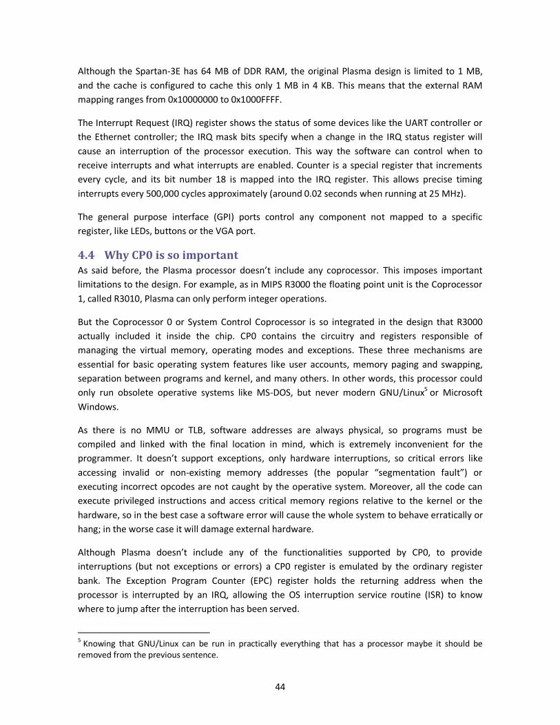
44
Although the Spartan-3E has 64 MB of DDR RAM, the original Plasma design is limited to 1 MB,
and the cache is configured to cache this only 1 MB in 4 KB. This means that the external RAM
mapping ranges from 0x10000000 to 0x1000FFFF.
The Interrupt Request (IRQ) register shows the status of some devices like the UART controller or
the Ethernet controller; the IRQ mask bits specify when a change in the IRQ status register will
cause an interruption of the processor execution. This way the software can control when to
receive interrupts and what interrupts are enabled. Counter is a special register that increments
every cycle, and its bit number 18 is mapped into the IRQ register. This allows precise timing
interrupts every 500,000 cycles approximately (around 0.02 seconds when running at 25 MHz).
The general purpose interface (GPI) ports control any component not mapped to a specific
register, like LEDs, buttons or the VGA port.
4.4 Why CP0 is so important As said before, the Plasma processor doesn’t include any coprocessor. This imposes important
limitations to the design. For example, as in MIPS R3000 the floating point unit is the Coprocessor
1, called R3010, Plasma can only perform integer operations.
But the Coprocessor 0 or System Control Coprocessor is so integrated in the design that R3000
actually included it inside the chip. CP0 contains the circuitry and registers responsible of
managing the virtual memory, operating modes and exceptions. These three mechanisms are
essential for basic operating system features like user accounts, memory paging and swapping,
separation between programs and kernel, and many others. In other words, this processor could
only run obsolete operative systems like MS-DOS, but never modern GNU/Linux5 or Microsoft
Windows.
As there is no MMU or TLB, software addresses are always physical, so programs must be
compiled and linked with the final location in mind, which is extremely inconvenient for the
programmer. It doesn’t support exceptions, only hardware interruptions, so critical errors like
accessing invalid or non-existing memory addresses (the popular “segmentation fault”) or
executing incorrect opcodes are not caught by the operative system. Moreover, all the code can
execute privileged instructions and access critical memory regions relative to the kernel or the
hardware, so in the best case a software error will cause the whole system to behave erratically or
hang; in the worse case it will damage external hardware.
Although Plasma doesn’t include any of the functionalities supported by CP0, to provide
interruptions (but not exceptions or errors) a CP0 register is emulated by the ordinary register
bank. The Exception Program Counter (EPC) register holds the returning address when the
processor is interrupted by an IRQ, allowing the OS interruption service routine (ISR) to know
where to jump after the interruption has been served.
5 Knowing that GNU/Linux can be run in practically everything that has a processor maybe it should be removed from the previous sentence.
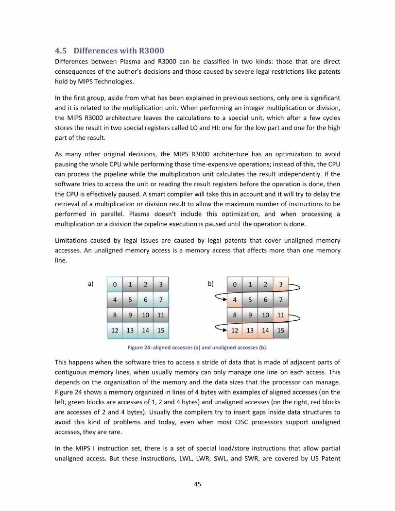
45
4.5 Differences with R3000 Differences between Plasma and R3000 can be classified in two kinds: those that are direct
consequences of the author’s decisions and those caused by severe legal restrictions like patents
hold by MIPS Technologies.
In the first group, aside from what has been explained in previous sections, only one is significant
and it is related to the multiplication unit. When performing an integer multiplication or division,
the MIPS R3000 architecture leaves the calculations to a special unit, which after a few cycles
stores the result in two special registers called LO and HI: one for the low part and one for the high
part of the result.
As many other original decisions, the MIPS R3000 architecture has an optimization to avoid
pausing the whole CPU while performing those time-expensive operations; instead of this, the CPU
can process the pipeline while the multiplication unit calculates the result independently. If the
software tries to access the unit or reading the result registers before the operation is done, then
the CPU is effectively paused. A smart compiler will take this in account and it will try to delay the
retrieval of a multiplication or division result to allow the maximum number of instructions to be
performed in parallel. Plasma doesn’t include this optimization, and when processing a
multiplication or a division the pipeline execution is paused until the operation is done.
Limitations caused by legal issues are caused by legal patents that cover unaligned memory
accesses. An unaligned memory access is a memory access that affects more than one memory
line.
Figure 24: aligned accesses (a) and unaligned accesses (b).
This happens when the software tries to access a stride of data that is made of adjacent parts of
contiguous memory lines, when usually memory can only manage one line on each access. This
depends on the organization of the memory and the data sizes that the processor can manage.
Figure 24 shows a memory organized in lines of 4 bytes with examples of aligned accesses (on the
left, green blocks are accesses of 1, 2 and 4 bytes) and unaligned accesses (on the right, red blocks
are accesses of 2 and 4 bytes). Usually the compilers try to insert gaps inside data structures to
avoid this kind of problems and today, even when most CISC processors support unaligned
accesses, they are rare.
In the MIPS I instruction set, there is a set of special load/store instructions that allow partial
unaligned access. But these instructions, LWL, LWR, SWL, and SWR, are covered by US Patent
0 1 2 3
4 5 6 7
8 9 10 11
12 13 14 15
0 1 2 3
4 5 6 7
8 9 10 11
12 13 14 15
a) b)

46
number 4,814,976 (Hansen, et al., 1989). However, this patent expired on December 23, 2006
(unfortunately 5 years after the Plasma design was started), so these instructions could be now
supported by Plasma.
47
5 The Honeycomb processor
This project aims to build a flexible multiprocessor architecture that could be run on an FPGA
platform. The Plasma processor was chosen to be the processing element of the system because it
had several advantages: it is compatible with a real, fairly used architecture as MIPS R3000; it is a
simple and small RISC implementation; and it is available in the public domain. But it lacked of a
few features, as explained in the previous chapter, which could compromise the suitability of the
system.
In this chapter a version of Plasma with integrated Coprocessor 0 is presented. This extended
design has been called Honeycomb.
5.1 Coprocessor 0 The integrated System Control Coprocessor or Coprocessor 0 is defined in the MIPS standard as a
logically separated unit with its own registers and pipeline. In the original design only one of CP0’s
registers was implemented. It was the Exception Program Counter (EPC) register, needed to
provide interruption support, and it was stored with ordinary general registers in the CPU’s
register bank.
To implement a real CP0 unit the whole set of registers had to be added and the data path had to
be separated from the processing register bank. The EPC register was moved to this new unit and
the data path between the control unit and the register bank was intercepted in a way that
accesses to EPC and other CP0 registers were managed no more by the register bank. Figure 25
shows the CPU in black and the CP0 in red.
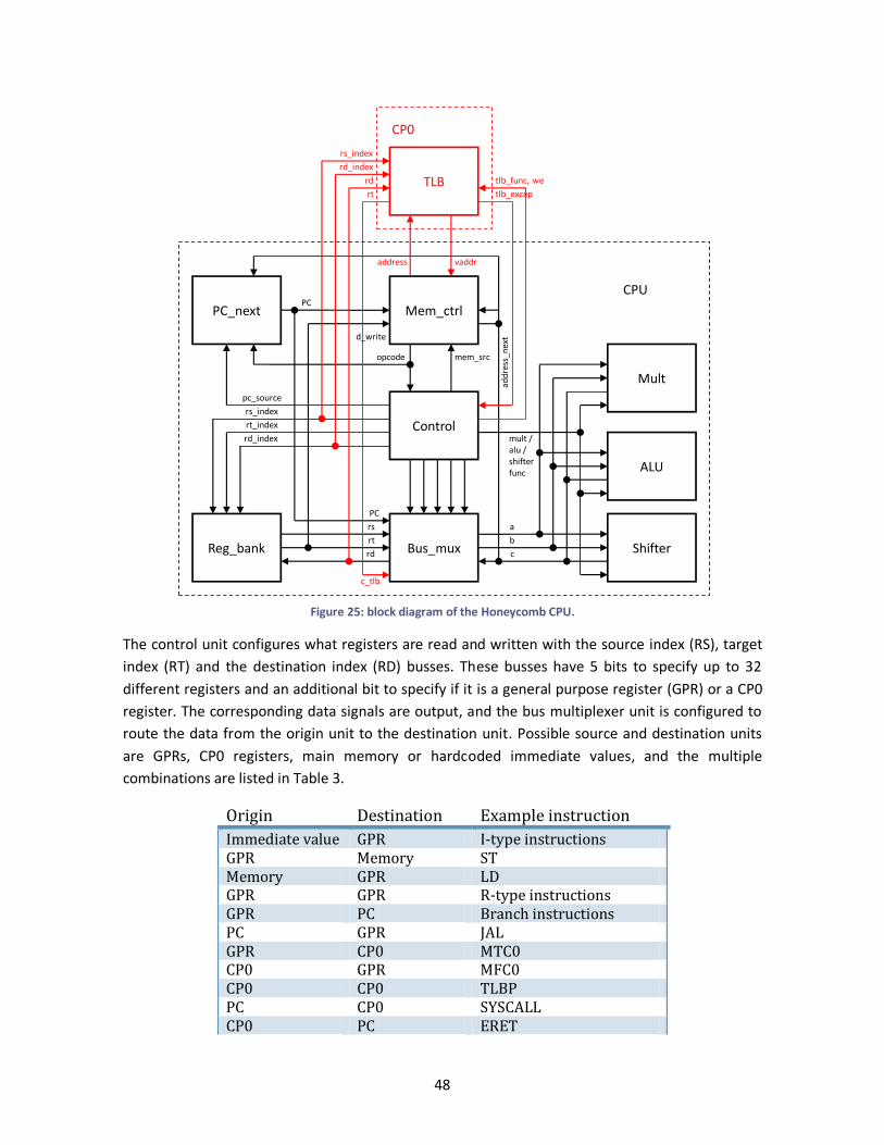
48
Figure 25: block diagram of the Honeycomb CPU.
The control unit configures what registers are read and written with the source index (RS), target
index (RT) and the destination index (RD) busses. These busses have 5 bits to specify up to 32
different registers and an additional bit to specify if it is a general purpose register (GPR) or a CP0
register. The corresponding data signals are output, and the bus multiplexer unit is configured to
route the data from the origin unit to the destination unit. Possible source and destination units
are GPRs, CP0 registers, main memory or hardcoded immediate values, and the multiple
combinations are listed in Table 3.
Origin Destination Example instruction
Immediate value GPR I-type instructions GPR Memory ST Memory GPR LD GPR GPR R-type instructions GPR PC Branch instructions PC GPR JAL GPR CP0 MTC0 CP0 GPR MFC0 CP0 CP0 TLBP PC CP0 SYSCALL CP0 PC ERET
PC_next Mem_ctrl
TLB
Control
Mult
ALU
ShifterBus_muxReg_bank
CP0
CPUPC
d_write
rs_index
rd_index
rd
rt
tlb_func, we
tlb_excep
address vaddr
rs_index
rt_index
rd_index
PC
rs
rt
rd
c_tlb
pc_source
opcode mem_src
a
b
c
mult /alu /shifterfunc
add
ress
_nex
t
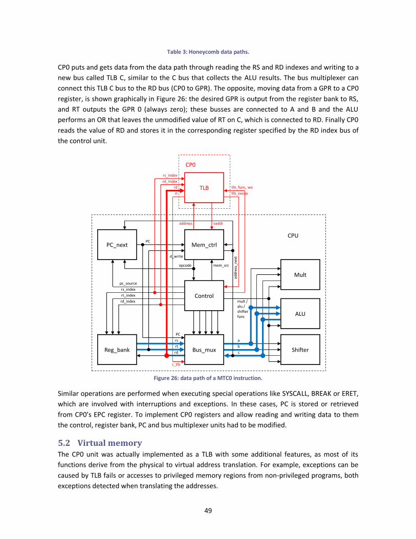
49
Table 3: Honeycomb data paths.
CP0 puts and gets data from the data path through reading the RS and RD indexes and writing to a
new bus called TLB C, similar to the C bus that collects the ALU results. The bus multiplexer can
connect this TLB C bus to the RD bus (CP0 to GPR). The opposite, moving data from a GPR to a CP0
register, is shown graphically in Figure 26: the desired GPR is output from the register bank to RS,
and RT outputs the GPR 0 (always zero); these busses are connected to A and B and the ALU
performs an OR that leaves the unmodified value of RT on C, which is connected to RD. Finally CP0
reads the value of RD and stores it in the corresponding register specified by the RD index bus of
the control unit.
Figure 26: data path of a MTC0 instruction.
Similar operations are performed when executing special operations like SYSCALL, BREAK or ERET,
which are involved with interruptions and exceptions. In these cases, PC is stored or retrieved
from CP0’s EPC register. To implement CP0 registers and allow reading and writing data to them
the control, register bank, PC and bus multiplexer units had to be modified.
5.2 Virtual memory The CP0 unit was actually implemented as a TLB with some additional features, as most of its
functions derive from the physical to virtual address translation. For example, exceptions can be
caused by TLB fails or accesses to privileged memory regions from non-privileged programs, both
exceptions detected when translating the addresses.
PC_next Mem_ctrl
TLB
Control
Mult
Shifter
CP0
CPUPC
d_write
rs_index
rd_index
rd
rt
tlb_func, we
tlb_excep
address vaddr
rs_index
rt_index
rd_index
PC
rs
rt
rd
c_tlb
pc_source
opcode mem_src
a
b
c
mult /alu /shifterfunc
add
ress
_nex
t
ALU
Bus_muxReg_bank
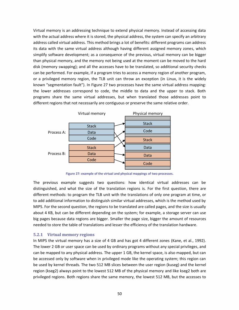
50
Virtual memory is an addressing technique to extend physical memory. Instead of accessing data
with the actual address where it is stored, the physical address, the system can specify an arbitrary
address called virtual address. This method brings a lot of benefits: different programs can address
its data with the same virtual address although having different assigned memory zones, which
simplify software development; as a consequence of the previous, virtual memory can be bigger
than physical memory, and the memory not being used at the moment can be moved to the hard
disk (memory swapping); and all the accesses have to be translated, so additional security checks
can be performed. For example, if a program tries to access a memory region of another program,
or a privileged memory region, the TLB unit can throw an exception (in Linux, it is the widely
known “segmentation fault”). In Figure 27 two processes have the same virtual address mapping:
the lower addresses correspond to code, the middle to data and the upper to stack. Both
programs share the same virtual addresses, but when translated those addresses point to
different regions that not necessarily are contiguous or preserve the same relative order.
Figure 27: example of the virtual and physical mappings of two processes.
The previous example suggests two questions: how identical virtual addresses can be
distinguished, and what the size of the translation regions is. For the first question, there are
different methods: to program the TLB unit with the translations of only one program at time, or
to add additional information to distinguish similar virtual addresses, which is the method used by
MIPS. For the second question, the regions to be translated are called pages, and the size is usually
about 4 KB, but can be different depending on the system; for example, a storage server can use
big pages because data regions are bigger. Smaller the page size, bigger the amount of resources
needed to store the table of translations and lesser the efficiency of the translation hardware.
5.2.1 Virtual memory regions
In MIPS the virtual memory has a size of 4 GB and has got 4 different zones (Kane, et al., 1992).
The lower 2 GB or user space can be used by ordinary programs without any special privileges, and
can be mapped to any physical address. The upper 1 GB, the kernel space, is also mapped, but can
be accessed only by software when in privileged mode like the operating system; this region can
be used by kernel threads. The two 512 MB slices between the user region (kuseg) and the kernel
region (kseg2) always point to the lowest 512 MB of the physical memory and like kseg2 both are
privileged regions. Both regions share the same memory, the lowest 512 MB, but the accesses to
Stack
Data
Virtual memory Physical memory
Code
Stack
Data
Code
Stack
Data
Code
Stack
Data
Code
Process A:
Process B:
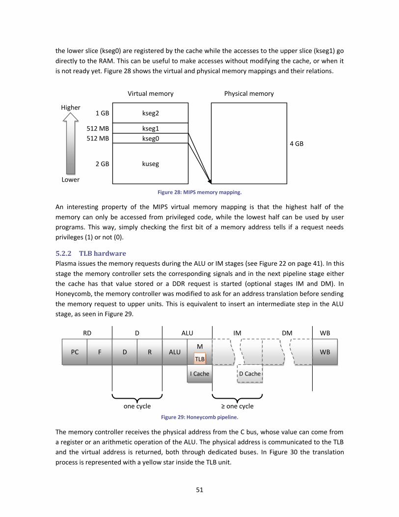
51
the lower slice (kseg0) are registered by the cache while the accesses to the upper slice (kseg1) go
directly to the RAM. This can be useful to make accesses without modifying the cache, or when it
is not ready yet. Figure 28 shows the virtual and physical memory mappings and their relations.
Figure 28: MIPS memory mapping.
An interesting property of the MIPS virtual memory mapping is that the highest half of the
memory can only be accessed from privileged code, while the lowest half can be used by user
programs. This way, simply checking the first bit of a memory address tells if a request needs
privileges (1) or not (0).
5.2.2 TLB hardware
Plasma issues the memory requests during the ALU or IM stages (see Figure 22 on page 41). In this
stage the memory controller sets the corresponding signals and in the next pipeline stage either
the cache has that value stored or a DDR request is started (optional stages IM and DM). In
Honeycomb, the memory controller was modified to ask for an address translation before sending
the memory request to upper units. This is equivalent to insert an intermediate step in the ALU
stage, as seen in Figure 29.
Figure 29: Honeycomb pipeline.
The memory controller receives the physical address from the C bus, whose value can come from
a register or an arithmetic operation of the ALU. The physical address is communicated to the TLB
and the virtual address is returned, both through dedicated buses. In Figure 30 the translation
process is represented with a yellow star inside the TLB unit.
RD
one cycle
D ALU IM WB
PC F ALU M
D R WB
DM
D Cache
≥ one cycle
TLB
I Cache
1 GB kseg2
kseg1
kseg0
kuseg
Virtual memory Physical memory
512 MB
4 GB
2 GB
512 MB
Lower
Higher
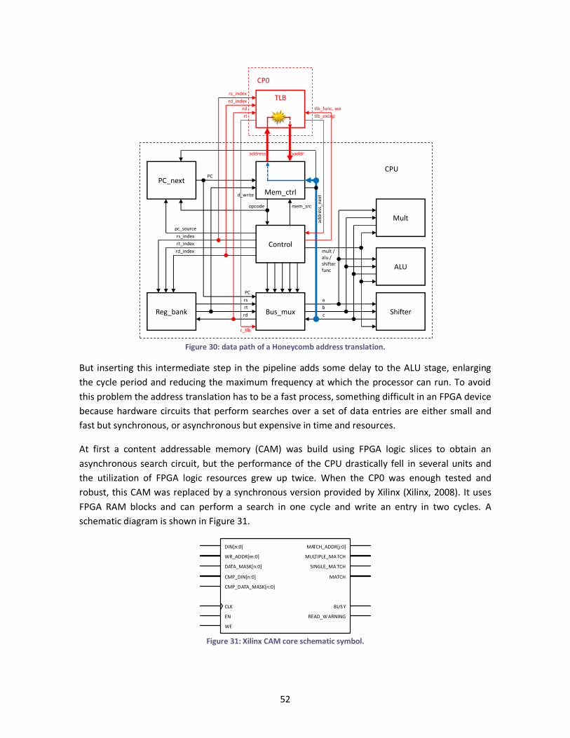
52
Figure 30: data path of a Honeycomb address translation.
But inserting this intermediate step in the pipeline adds some delay to the ALU stage, enlarging
the cycle period and reducing the maximum frequency at which the processor can run. To avoid
this problem the address translation has to be a fast process, something difficult in an FPGA device
because hardware circuits that perform searches over a set of data entries are either small and
fast but synchronous, or asynchronous but expensive in time and resources.
At first a content addressable memory (CAM) was build using FPGA logic slices to obtain an
asynchronous search circuit, but the performance of the CPU drastically fell in several units and
the utilization of FPGA logic resources grew up twice. When the CP0 was enough tested and
robust, this CAM was replaced by a synchronous version provided by Xilinx (Xilinx, 2008). It uses
FPGA RAM blocks and can perform a search in one cycle and write an entry in two cycles. A
schematic diagram is shown in Figure 31.
Figure 31: Xilinx CAM core schematic symbol.
PC_next
Mem_ctrl
TLB
Control
Mult
ALU
ShifterBus_muxReg_bank
CP0
CPUPC
d_write
rs_index
rd_index
rd
rt
tlb_func, we
tlb_excep
address vaddr
rs_index
rt_index
rd_index
PC
rs
rt
rd
c_tlb
pc_source
opcode mem_src
a
b
c
mult /alu /shifterfunc
add
ress
_nex
t
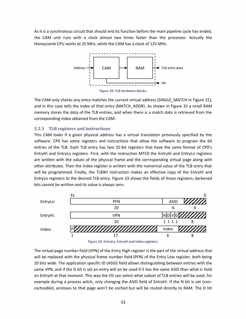
53
As it is a synchronous circuit that should end its function before the main pipeline cycle has ended,
the CAM unit runs with a clock almost two times faster than the processor. Actually the
Honeycomb CPU works at 25 MHz, while the CAM has a clock of 125 MHz.
Figure 32: TLB hardware blocks.
The CAM only checks any entry matches the current virtual address (SINGLE_MATCH in Figure 31),
and in this case tells the index of that entry (MATCH_ADDR). As shown in Figure 32 a small RAM
memory stores the data of the TLB entries, and when there is a match data is retrieved from the
corresponding index obtained from the CAM.
5.2.3 TLB registers and instructions
This CAM looks if a given physical address has a virtual translation previously specified by the
software. CP0 has some registers and instructions that allow the software to program the 64
entries of the TLB. Each TLB entry has two 32-bit registers that have the same format of CP0’s
EntryHi and EntryLo registers. First, with the instruction MTC0 the EntryHi and EntryLo registers
are written with the values of the physical frame and the corresponding virtual page along with
other attributes. Then the Index register is written with the numerical value of the TLB entry that
will be programmed. Finally, the TLBWI instruction makes an effective copy of the EntryHi and
EntryLo registers to the desired TLB entry. Figure 33 shows the fields of those registers; darkened
bits cannot be written and its value is always zero.
Figure 33: EntryLo, EntryHi and Index registers.
The virtual page number field (VPN) of the Entry High register is the part of the virtual address that
will be replaced with the physical frame number field (PFN) of the Entry Low register, both being
20 bits wide. The application specific ID (ASID) field allows distinguishing between entries with the
same VPN, and if the G bit is set an entry will on be used if it has the same ASID than what is hold
on EntryHi at that moment. This way the OS can select what subset of TLB entries will be used, for
example during a process witch, only changing the ASID field of EntryHi. If the N bit is set (non-
cacheable), accesses to that page won’t be cached but will be routed directly to RAM. The D bit
31 0
PFN ASID EntryLo:
6 6 20
EntryHi: VPN
8 1 20
N D V G
1 1 1
Index: Index
P
1 17 8 6
CAM RAM Address TLB entry data
Hit
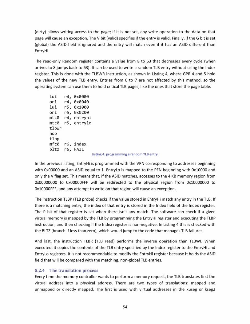
54
(dirty) allows writing access to the page; if it is not set, any write operation to the data on that
page will cause an exception. The V bit (valid) specifies if the entry is valid. Finally, if the G bit is set
(global) the ASID field is ignored and the entry will match even if it has an ASID different than
EntryHi.
The read-only Random register contains a value from 8 to 63 that decreases every cycle (when
arrives to 8 jumps back to 63). It can be used to write a random TLB entry without using the Index
register. This is done with the TLBWR instruction, as shown in Listing 4, where GPR 4 and 5 hold
the values of the new TLB entry. Entries from 0 to 7 are not affected by this method, so the
operating system can use them to hold critical TLB pages, like the ones that store the page table.
lui r4, 0x0000 ori r4, 0x0040 lui r5, 0x1000 ori r5, 0x0200 mtc0 r4, entryhi mtc0 r5, entrylo tlbwr nop tlbp mfc0 r6, index bltz r6, FAIL
Listing 4: programming a random TLB entry.
In the previous listing, EntryHi is programmed with the VPN corresponding to addresses beginning
with 0x00000 and an ASID equal to 1. EntryLo is mapped to the PFN beginning with 0x10000 and
only the V flag set. This means that, if the ASID matches, accesses to the 4 KB memory region from
0x00000000 to 0x00000FFF will be redirected to the physical region from 0x10000000 to
0x10000FFF, and any attempt to write on that region will cause an exception.
The instruction TLBP (TLB probe) checks if the value stored in EntryHi match any entry in the TLB. If
there is a matching entry, the index of that entry is stored in the Index field of the Index register.
The P bit of that register is set when there isn’t any match. The software can check if a given
virtual memory is mapped by the TLB by programming the EntryHi register and executing the TLBP
instruction, and then checking if the Index register is non-negative. In Listing 4 this is checked with
the BLTZ (branch if less than zero), which would jump to the code that manages TLB failures.
And last, the instruction TLBR (TLB read) performs the inverse operation than TLBWI. When
executed, it copies the contents of the TLB entry specified by the Index register to the EntryHi and
EntryLo registers. It is not recommendable to modify the EntryHi register because it holds the ASID
field that will be compared with the matching, non-global TLB entries.
5.2.4 The translation process
Every time the memory controller wants to perform a memory request, the TLB translates first the
virtual address into a physical address. There are two types of translations: mapped and
unmapped or directly mapped. The first is used with virtual addresses in the kuseg or kseg2
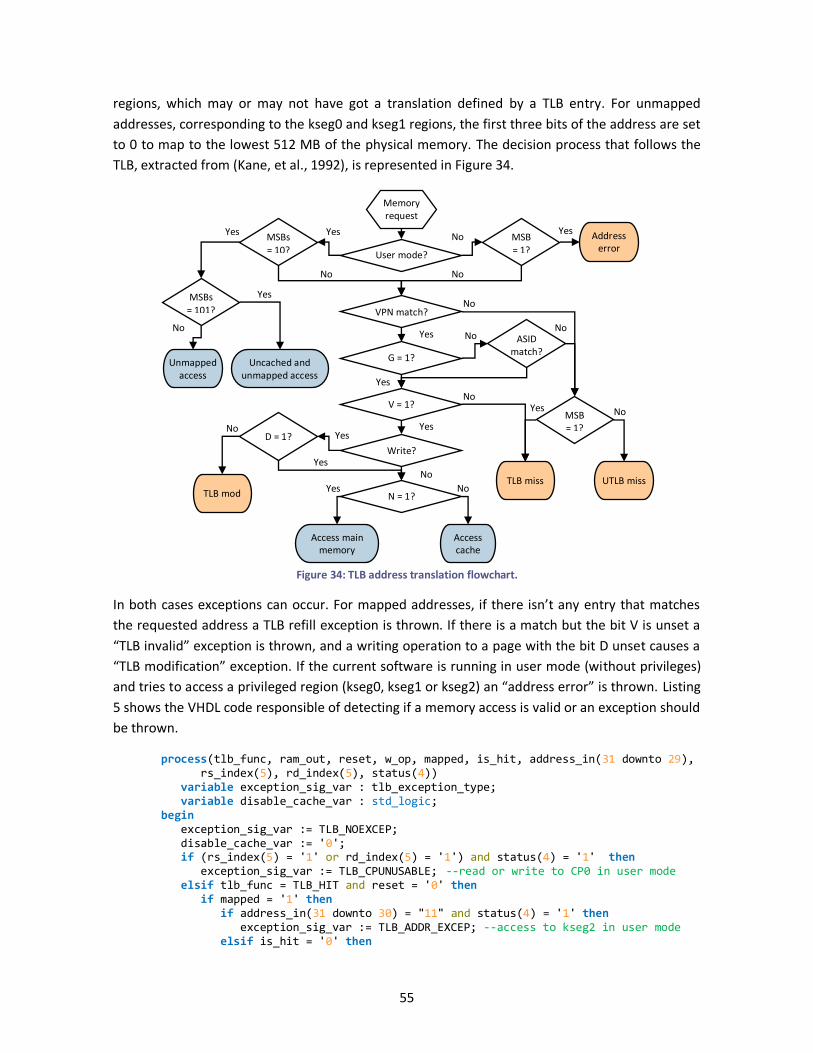
55
regions, which may or may not have got a translation defined by a TLB entry. For unmapped
addresses, corresponding to the kseg0 and kseg1 regions, the first three bits of the address are set
to 0 to map to the lowest 512 MB of the physical memory. The decision process that follows the
TLB, extracted from (Kane, et al., 1992), is represented in Figure 34.
Figure 34: TLB address translation flowchart.
In both cases exceptions can occur. For mapped addresses, if there isn’t any entry that matches
the requested address a TLB refill exception is thrown. If there is a match but the bit V is unset a
“TLB invalid” exception is thrown, and a writing operation to a page with the bit D unset causes a
“TLB modification” exception. If the current software is running in user mode (without privileges)
and tries to access a privileged region (kseg0, kseg1 or kseg2) an “address error” is thrown. Listing
5 shows the VHDL code responsible of detecting if a memory access is valid or an exception should
be thrown.
process(tlb_func, ram_out, reset, w_op, mapped, is_hit, address_in(31 downto 29), rs_index(5), rd_index(5), status(4)) variable exception_sig_var : tlb_exception_type; variable disable_cache_var : std_logic; begin exception_sig_var := TLB_NOEXCEP; disable_cache_var := '0'; if (rs_index(5) = '1' or rd_index(5) = '1') and status(4) = '1' then exception_sig_var := TLB_CPUNUSABLE; --read or write to CP0 in user mode elsif tlb_func = TLB_HIT and reset = '0' then if mapped = '1' then if address_in(31 downto 30) = "11" and status(4) = '1' then exception_sig_var := TLB_ADDR_EXCEP; --access to kseg2 in user mode elsif is_hit = '0' then
Memory request
User mode?
MSB = 1?
Address error
VPN match?
G = 1?
V = 1?
Write?
N = 1?
Access main memory
Access cache
MSBs = 10?
Unmapped access
ASID match?
MSB = 1?
TLB miss UTLB miss
D = 1?
TLB mod
Yes Yes
No No
No
No No
No
No
Yes
Yes
No
No
Yes
Yes
Yes
No
Yes
No
Yes
Yes
MSBs = 101?
Uncached and unmapped access
Yes
No
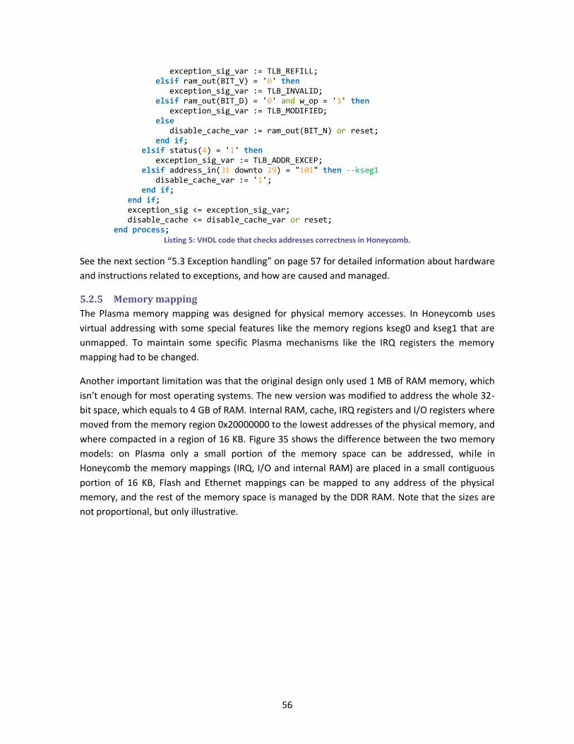
56
exception_sig_var := TLB_REFILL; elsif ram_out(BIT_V) = '0' then exception_sig_var := TLB_INVALID; elsif ram_out(BIT_D) = '0' and w_op = '1' then exception_sig_var := TLB_MODIFIED; else disable_cache_var := ram_out(BIT_N) or reset; end if; elsif status(4) = '1' then exception_sig_var := TLB_ADDR_EXCEP; elsif address_in(31 downto 29) = "101" then --kseg1 disable_cache_var := '1'; end if; end if; exception_sig <= exception_sig_var; disable_cache <= disable_cache_var or reset; end process;
Listing 5: VHDL code that checks addresses correctness in Honeycomb.
See the next section “5.3 Exception handling” on page 57 for detailed information about hardware
and instructions related to exceptions, and how are caused and managed.
5.2.5 Memory mapping
The Plasma memory mapping was designed for physical memory accesses. In Honeycomb uses
virtual addressing with some special features like the memory regions kseg0 and kseg1 that are
unmapped. To maintain some specific Plasma mechanisms like the IRQ registers the memory
mapping had to be changed.
Another important limitation was that the original design only used 1 MB of RAM memory, which
isn’t enough for most operating systems. The new version was modified to address the whole 32-
bit space, which equals to 4 GB of RAM. Internal RAM, cache, IRQ registers and I/O registers where
moved from the memory region 0x20000000 to the lowest addresses of the physical memory, and
where compacted in a region of 16 KB. Figure 35 shows the difference between the two memory
models: on Plasma only a small portion of the memory space can be addressed, while in
Honeycomb the memory mappings (IRQ, I/O and internal RAM) are placed in a small contiguous
portion of 16 KB, Flash and Ethernet mappings can be mapped to any address of the physical
memory, and the rest of the memory space is managed by the DDR RAM. Note that the sizes are
not proportional, but only illustrative.
57
Figure 35: comparison between Plasma and Honeycomb memory mappings.
The actual addresses of I/O ports and other memory mappings can be found in Table 4. The lower
16 KB can be accessed through the unmapped memory regions kseg0 or kseg1 just adding
0x800000000 or 0xA0000000 to the address, respectively. Ethernet DMA regions and the Flash
memory mapping don’t have a fixed address, but can be mapped by the software.
Address Description Size
0x0000 0000 Internal RAM 4 KB 0x0000 1000 Cache contents 4 KB
0x0000 0000 UART read/write 32 bits 0x0000 0010 IRQ mask 32 bits 0x0000 0020 IRQ status 32 bits 0x0000 0030 GPI output set bits 32 bits 0x0000 0040 GPI output clear bits 32 bits 0x0000 0050 GPI input 32 bits 0x0000 0060 Counter 32 bits 0x0000 0070 Ethernet transmit count 32 bits 0x0000 00A0 CPUID 32 bits
… ? Ethernet sending DMA region 64 KB ? Ethernet receiving DMA region 64 KB ? Flash memory Up to 64 MB
Table 4: Honeycomb memory mapping.
The rest of the address space is considered as DDR RAM. A new register was introduced called
CPUID that contains the number of the core. This is useful for multiprocessors that need to
distinguish between different cores.
5.3 Exception handling Plasma had interruption support for hardware IRQs, like a simple clock, Ethernet, Flash or UART.
But in MIPS, interrupts differ from exceptions, and even from errors. Interrupts are external
signals that the processor usually can ignore and process when it considers it is the best moment.
For example, in Plasma an interrupt cannot be processed during a branch slot because the
returning address could be wrong.
Unused memory
Internal RAM + cache
IRQ + I/O
DDR
Ethernet
Flash
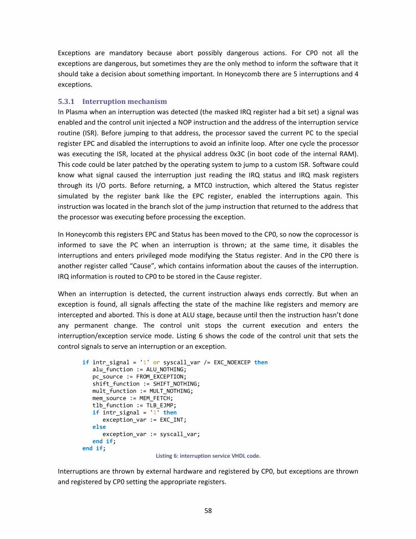
58
Exceptions are mandatory because abort possibly dangerous actions. For CP0 not all the
exceptions are dangerous, but sometimes they are the only method to inform the software that it
should take a decision about something important. In Honeycomb there are 5 interruptions and 4
exceptions.
5.3.1 Interruption mechanism
In Plasma when an interruption was detected (the masked IRQ register had a bit set) a signal was
enabled and the control unit injected a NOP instruction and the address of the interruption service
routine (ISR). Before jumping to that address, the processor saved the current PC to the special
register EPC and disabled the interruptions to avoid an infinite loop. After one cycle the processor
was executing the ISR, located at the physical address 0x3C (in boot code of the internal RAM).
This code could be later patched by the operating system to jump to a custom ISR. Software could
know what signal caused the interruption just reading the IRQ status and IRQ mask registers
through its I/O ports. Before returning, a MTC0 instruction, which altered the Status register
simulated by the register bank like the EPC register, enabled the interruptions again. This
instruction was located in the branch slot of the jump instruction that returned to the address that
the processor was executing before processing the exception.
In Honeycomb this registers EPC and Status has been moved to the CP0, so now the coprocessor is
informed to save the PC when an interruption is thrown; at the same time, it disables the
interruptions and enters privileged mode modifying the Status register. And in the CP0 there is
another register called “Cause”, which contains information about the causes of the interruption.
IRQ information is routed to CP0 to be stored in the Cause register.
When an interruption is detected, the current instruction always ends correctly. But when an
exception is found, all signals affecting the state of the machine like registers and memory are
intercepted and aborted. This is done at ALU stage, because until then the instruction hasn’t done
any permanent change. The control unit stops the current execution and enters the
interruption/exception service mode. Listing 6 shows the code of the control unit that sets the
control signals to serve an interruption or an exception.
if intr_signal = '1' or syscall_var /= EXC_NOEXCEP then alu_function := ALU_NOTHING; pc_source := FROM_EXCEPTION; shift_function := SHIFT_NOTHING; mult_function := MULT_NOTHING; mem_source := MEM_FETCH; tlb_function := TLB_EJMP; if intr_signal = '1' then exception_var := EXC_INT; else exception_var := syscall_var; end if; end if;
Listing 6: interruption service VHDL code.
Interruptions are thrown by external hardware and registered by CP0, but exceptions are thrown
and registered by CP0 setting the appropriate registers.
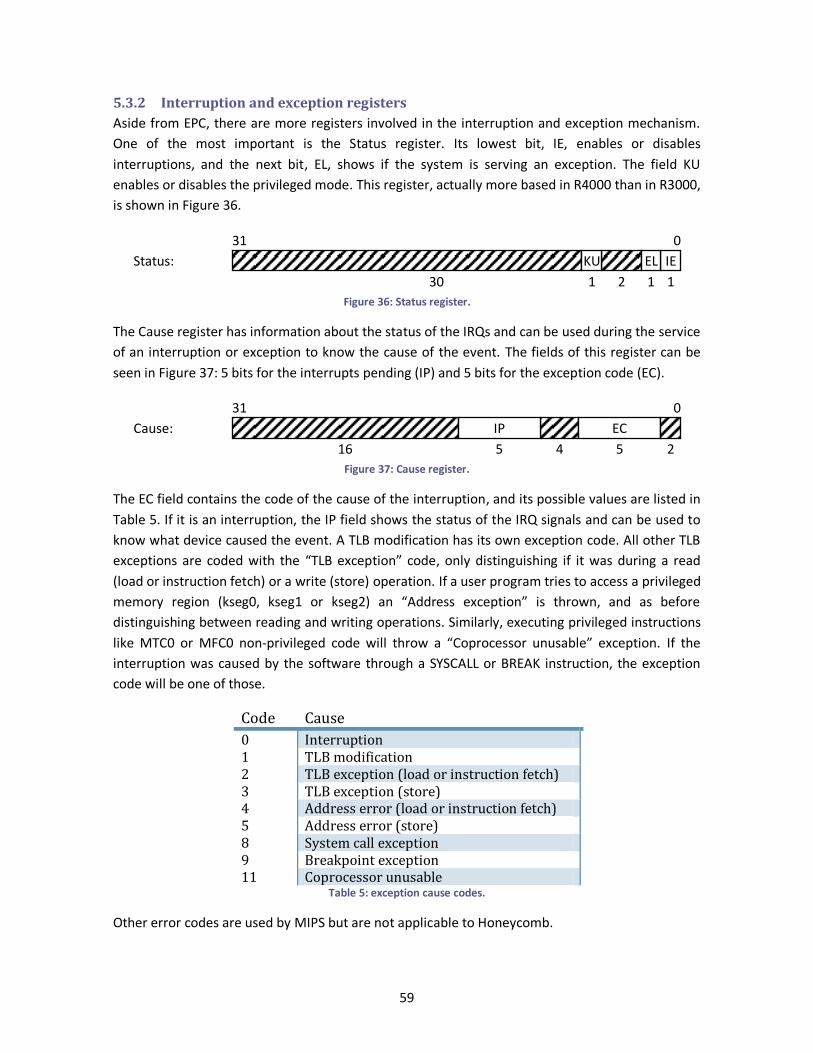
59
5.3.2 Interruption and exception registers
Aside from EPC, there are more registers involved in the interruption and exception mechanism.
One of the most important is the Status register. Its lowest bit, IE, enables or disables
interruptions, and the next bit, EL, shows if the system is serving an exception. The field KU
enables or disables the privileged mode. This register, actually more based in R4000 than in R3000,
is shown in Figure 36.
Figure 36: Status register.
The Cause register has information about the status of the IRQs and can be used during the service
of an interruption or exception to know the cause of the event. The fields of this register can be
seen in Figure 37: 5 bits for the interrupts pending (IP) and 5 bits for the exception code (EC).
Figure 37: Cause register.
The EC field contains the code of the cause of the interruption, and its possible values are listed in
Table 5. If it is an interruption, the IP field shows the status of the IRQ signals and can be used to
know what device caused the event. A TLB modification has its own exception code. All other TLB
exceptions are coded with the “TLB exception” code, only distinguishing if it was during a read
(load or instruction fetch) or a write (store) operation. If a user program tries to access a privileged
memory region (kseg0, kseg1 or kseg2) an “Address exception” is thrown, and as before
distinguishing between reading and writing operations. Similarly, executing privileged instructions
like MTC0 or MFC0 non-privileged code will throw a “Coprocessor unusable” exception. If the
interruption was caused by the software through a SYSCALL or BREAK instruction, the exception
code will be one of those.
Code Cause
0 Interruption 1 TLB modification 2 TLB exception (load or instruction fetch) 3 TLB exception (store) 4 Address error (load or instruction fetch) 5 Address error (store) 8 System call exception 9 Breakpoint exception 11 Coprocessor unusable
Table 5: exception cause codes.
Other error codes are used by MIPS but are not applicable to Honeycomb.
31 0
Cause:
2 16
EC
5
5
IP
4
31 0
Status:
1 30
IE EL
1
KU
1 2
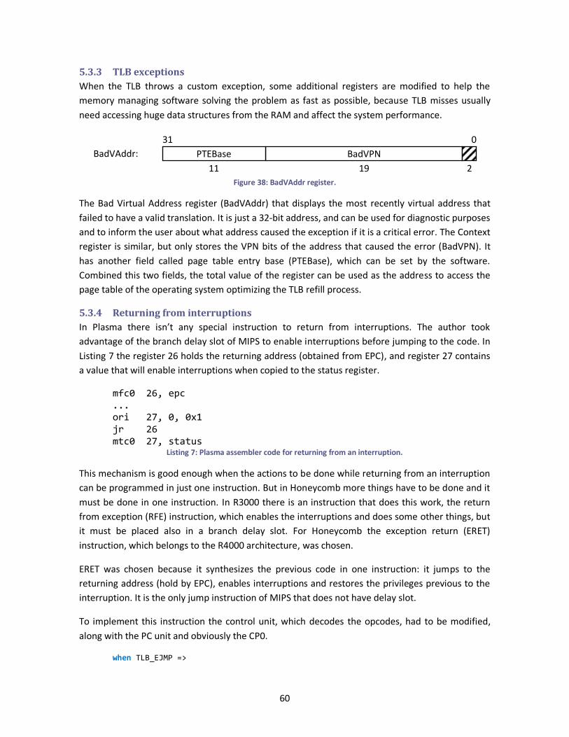
60
5.3.3 TLB exceptions
When the TLB throws a custom exception, some additional registers are modified to help the
memory managing software solving the problem as fast as possible, because TLB misses usually
need accessing huge data structures from the RAM and affect the system performance.
Figure 38: BadVAddr register.
The Bad Virtual Address register (BadVAddr) that displays the most recently virtual address that
failed to have a valid translation. It is just a 32-bit address, and can be used for diagnostic purposes
and to inform the user about what address caused the exception if it is a critical error. The Context
register is similar, but only stores the VPN bits of the address that caused the error (BadVPN). It
has another field called page table entry base (PTEBase), which can be set by the software.
Combined this two fields, the total value of the register can be used as the address to access the
page table of the operating system optimizing the TLB refill process.
5.3.4 Returning from interruptions
In Plasma there isn’t any special instruction to return from interruptions. The author took
advantage of the branch delay slot of MIPS to enable interruptions before jumping to the code. In
Listing 7 the register 26 holds the returning address (obtained from EPC), and register 27 contains
a value that will enable interruptions when copied to the status register.
mfc0 26, epc ... ori 27, 0, 0x1 jr 26 mtc0 27, status
Listing 7: Plasma assembler code for returning from an interruption.
This mechanism is good enough when the actions to be done while returning from an interruption
can be programmed in just one instruction. But in Honeycomb more things have to be done and it
must be done in one instruction. In R3000 there is an instruction that does this work, the return
from exception (RFE) instruction, which enables the interruptions and does some other things, but
it must be placed also in a branch delay slot. For Honeycomb the exception return (ERET)
instruction, which belongs to the R4000 architecture, was chosen.
ERET was chosen because it synthesizes the previous code in one instruction: it jumps to the
returning address (hold by EPC), enables interruptions and restores the privileges previous to the
interruption. It is the only jump instruction of MIPS that does not have delay slot.
To implement this instruction the control unit, which decodes the opcodes, had to be modified,
along with the PC unit and obviously the CP0.
when TLB_EJMP =>
31 0
BadVAddr:
2 11
BadVPN
19
PTEBase
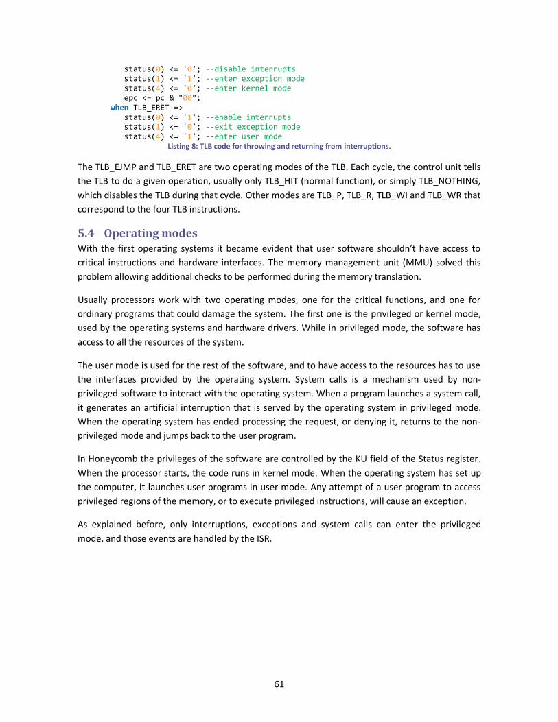
61
status(0) <= '0'; --disable interrupts status(1) <= '1'; --enter exception mode status(4) <= '0'; --enter kernel mode epc <= pc & "00"; when TLB_ERET => status(0) <= '1'; --enable interrupts status(1) <= '0'; --exit exception mode status(4) <= '1'; --enter user mode
Listing 8: TLB code for throwing and returning from interruptions.
The TLB_EJMP and TLB_ERET are two operating modes of the TLB. Each cycle, the control unit tells
the TLB to do a given operation, usually only TLB_HIT (normal function), or simply TLB_NOTHING,
which disables the TLB during that cycle. Other modes are TLB_P, TLB_R, TLB_WI and TLB_WR that
correspond to the four TLB instructions.
5.4 Operating modes With the first operating systems it became evident that user software shouldn’t have access to
critical instructions and hardware interfaces. The memory management unit (MMU) solved this
problem allowing additional checks to be performed during the memory translation.
Usually processors work with two operating modes, one for the critical functions, and one for
ordinary programs that could damage the system. The first one is the privileged or kernel mode,
used by the operating systems and hardware drivers. While in privileged mode, the software has
access to all the resources of the system.
The user mode is used for the rest of the software, and to have access to the resources has to use
the interfaces provided by the operating system. System calls is a mechanism used by non-
privileged software to interact with the operating system. When a program launches a system call,
it generates an artificial interruption that is served by the operating system in privileged mode.
When the operating system has ended processing the request, or denying it, returns to the non-
privileged mode and jumps back to the user program.
In Honeycomb the privileges of the software are controlled by the KU field of the Status register.
When the processor starts, the code runs in kernel mode. When the operating system has set up
the computer, it launches user programs in user mode. Any attempt of a user program to access
privileged regions of the memory, or to execute privileged instructions, will cause an exception.
As explained before, only interruptions, exceptions and system calls can enter the privileged
mode, and those events are handled by the ISR.
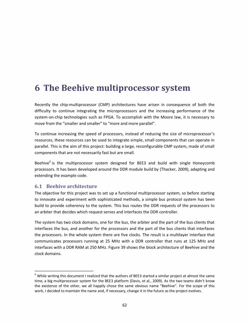
62
6 The Beehive multiprocessor system
Recently the chip-multiprocessor (CMP) architectures have arisen in consequence of both the
difficulty to continue integrating the microprocessors and the increasing performance of the
system-on-chip technologies such as FPGA. To accomplish with the Moore law, it is necessary to
move from the “smaller and smaller” to “more and more parallel”.
To continue increasing the speed of processors, instead of reducing the size of microprocessor’s
resources, these resources can be used to integrate simple, small components that can operate in
parallel. This is the aim of this project: building a large, reconfigurable CMP system, made of small
components that are not necessarily fast but are small.
Beehive6 is the multiprocessor system designed for BEE3 and build with single Honeycomb
processors. It has been developed around the DDR module build by (Thacker, 2009), adapting and
extending the example code.
6.1 Beehive architecture The objective for this project was to set up a functional multiprocessor system, so before starting
to innovate and experiment with sophisticated methods, a simple bus protocol system has been
build to provide coherency to the system. This bus routes the DDR requests of the processors to
an arbiter that decides which request serves and interfaces the DDR controller.
The system has two clock domains, one for the bus, the arbiter and the part of the bus clients that
interfaces the bus, and another for the processors and the part of the bus clients that interfaces
the processors. In the whole system there are five clocks. The result is a multilayer interface that
communicates processors running at 25 MHz with a DDR controller that runs at 125 MHz and
interfaces with a DDR RAM at 250 MHz. Figure 39 shows the block architecture of Beehive and the
clock domains.
6 While writing this document I realized that the authors of BEE3 started a similar project at almost the same time, a big multiprocessor system for the BEE3 platform (Davis, et al., 2009). As the two teams didn’t know the existence of the other, we all happily chose the same obvious name “Beehive”. For the scope of this work, I decided to maintain the name and, if necessary, change it in the future as the project evolves.
63
Figure 39: Beehive architecture.
This high complexity is due to various reasons. The terminal components of the bus system, the
DDR controller and the Honeycomb processor, are designed to work at a given speed. Honeycomb
is an extension of the Plasma processor, which emulates the MIPS R3000 that run at 25 MHz. The
DDR controller is fine-tuned to work with a DDR2-500 RAM and modifying the design can cause
fatal consequences.
To maintain the coherence between the different clock domains several finite state machines
(FSM) have been implemented. At each contact point between two clock domains, two FSM
synchronize the data exchange with handshaking mechanisms. This slows the performance, but
the main objective of this work is robustness rather than speed.
A minor detail that shows the complexity of merging several designs in a single system is the
difference in design methods. While Honeycomb is build in VHDL, like Plasma, the DDR controller,
the bus arbiter and the bus clients are written in Verilog. Although this and other difficulties can
be solved easily, the system is not as well designed as a system completely designed from scratch.
6.2 Honeycomb, the Beehive processor Several minor modifications had to be done to the Honeycomb processor before inserting it in the
Beehive system. First, a simple mechanism was included to allow the software distinguishing
between each processor.
A new register was added to the memory mapping with a unique 32-bit identifier. The current
system allows up to 256 processors, but this number can be increased with only some small
changes to the design.
Another problem was related with the way that the bus client detected the memory requests from
the processor. As Honeycomb maintained the read or write request raised during the whole
request, the new signal new_req was added. Its value is high during only one cycle at the
250 MHz 125 MHz
25 MHz
Bus arbiter Bus
Bus client
P
Bus client
P
Bus client
P
…
Bus client
P
… Bus client
P
Bus client
P
DDR controller
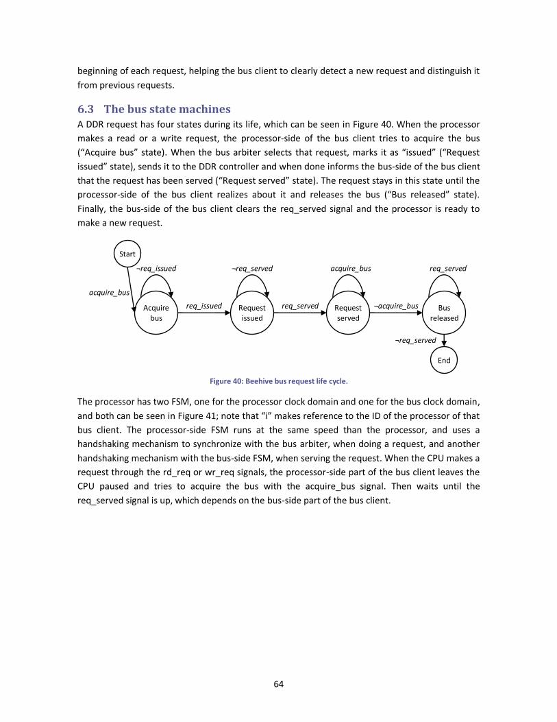
64
beginning of each request, helping the bus client to clearly detect a new request and distinguish it
from previous requests.
6.3 The bus state machines A DDR request has four states during its life, which can be seen in Figure 40. When the processor
makes a read or a write request, the processor-side of the bus client tries to acquire the bus
(“Acquire bus” state). When the bus arbiter selects that request, marks it as “issued” (“Request
issued” state), sends it to the DDR controller and when done informs the bus-side of the bus client
that the request has been served (“Request served” state). The request stays in this state until the
processor-side of the bus client realizes about it and releases the bus (“Bus released” state).
Finally, the bus-side of the bus client clears the req_served signal and the processor is ready to
make a new request.
Figure 40: Beehive bus request life cycle.
The processor has two FSM, one for the processor clock domain and one for the bus clock domain,
and both can be seen in Figure 41; note that “i” makes reference to the ID of the processor of that
bus client. The processor-side FSM runs at the same speed than the processor, and uses a
handshaking mechanism to synchronize with the bus arbiter, when doing a request, and another
handshaking mechanism with the bus-side FSM, when serving the request. When the CPU makes a
request through the rd_req or wr_req signals, the processor-side part of the bus client leaves the
CPU paused and tries to acquire the bus with the acquire_bus signal. Then waits until the
req_served signal is up, which depends on the bus-side part of the bus client.
Acquire bus
Request issued
Request served
Bus released
req_issued req_served ¬acquire_bus
¬req_issued ¬req_served acquire_bus req_served
¬req_served
Start
acquire_bus
End
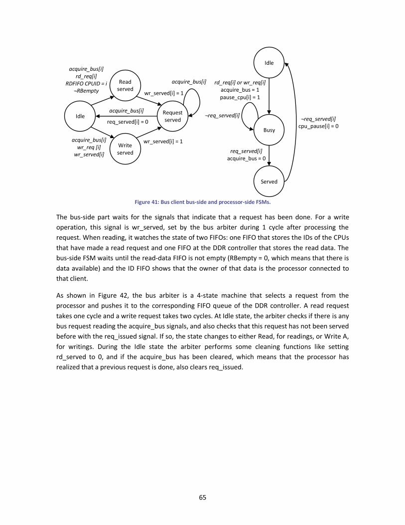
65
Figure 41: Bus client bus-side and processor-side FSMs.
The bus-side part waits for the signals that indicate that a request has been done. For a write
operation, this signal is wr_served, set by the bus arbiter during 1 cycle after processing the
request. When reading, it watches the state of two FIFOs: one FIFO that stores the IDs of the CPUs
that have made a read request and one FIFO at the DDR controller that stores the read data. The
bus-side FSM waits until the read-data FIFO is not empty (RBempty = 0, which means that there is
data available) and the ID FIFO shows that the owner of that data is the processor connected to
that client.
As shown in Figure 42, the bus arbiter is a 4-state machine that selects a request from the
processor and pushes it to the corresponding FIFO queue of the DDR controller. A read request
takes one cycle and a write request takes two cycles. At Idle state, the arbiter checks if there is any
bus request reading the acquire_bus signals, and also checks that this request has not been served
before with the req_issued signal. If so, the state changes to either Read, for readings, or Write A,
for writings. During the Idle state the arbiter performs some cleaning functions like setting
rd_served to 0, and if the acquire_bus has been cleared, which means that the processor has
realized that a previous request is done, also clears req_issued.
Idle
Read served
Write served
acquire_bus[i] wr_req [i]
wr_served[i]
acquire_bus[i] rd_req[i]
RDFIFO CPUID = i ¬RBempty wr_served[i] = 1
Request served
wr_served[i] = 1
acquire_bus[i]
req_served[i] = 0
acquire_bus[i]
Idle
Busy
Served
rd_req[i] or wr_req[i] acquire_bus = 1 pause_cpu[i] = 1
req_served[i] acquire_bus = 0
¬req_served[i] ¬req_served[i]
cpu_pause[i] = 0
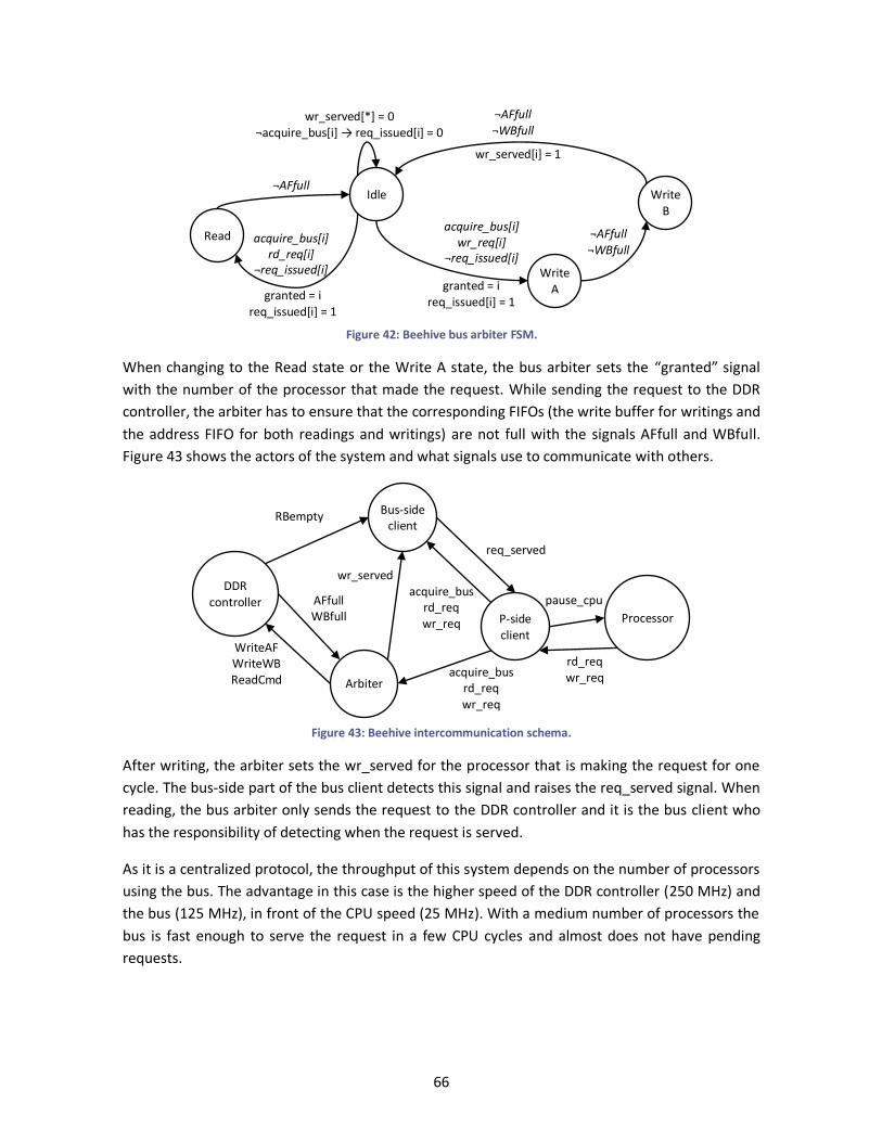
66
Figure 42: Beehive bus arbiter FSM.
When changing to the Read state or the Write A state, the bus arbiter sets the “granted” signal
with the number of the processor that made the request. While sending the request to the DDR
controller, the arbiter has to ensure that the corresponding FIFOs (the write buffer for writings and
the address FIFO for both readings and writings) are not full with the signals AFfull and WBfull.
Figure 43 shows the actors of the system and what signals use to communicate with others.
Figure 43: Beehive intercommunication schema.
After writing, the arbiter sets the wr_served for the processor that is making the request for one
cycle. The bus-side part of the bus client detects this signal and raises the req_served signal. When
reading, the bus arbiter only sends the request to the DDR controller and it is the bus client who
has the responsibility of detecting when the request is served.
As it is a centralized protocol, the throughput of this system depends on the number of processors
using the bus. The advantage in this case is the higher speed of the DDR controller (250 MHz) and
the bus (125 MHz), in front of the CPU speed (25 MHz). With a medium number of processors the
bus is fast enough to serve the request in a few CPU cycles and almost does not have pending
requests.
Arbiter
acquire_bus rd_req wr_req
Bus-side client
P-side client
req_served
wr_served
acquire_bus rd_req wr_req
DDR controller
Processor
WriteAF WriteWB ReadCmd
AFfull WBfull
RBempty
pause_cpu
rd_req wr_req
Idle
Write A
Write B
Read ¬AFfull ¬WBfull
¬AFfull ¬WBfull
acquire_bus[i] wr_req[i]
¬req_issued[i]
granted = i req_issued[i] = 1
wr_served[i] = 1
acquire_bus[i] rd_req[i]
¬req_issued[i]
granted = i req_issued[i] = 1
¬AFfull
wr_served[*] = 0 ¬acquire_bus[i] → req_issued[i] = 0
67
7 Conclusions
As a main conclusion, the system presented in this work accomplished with the basic objectives
proposed at the beginning. Some of the features planned like transactional memory support
couldn’t be developed, but the fundamental parts of a multiprocessing system have been
implemented.
Compared to other systems like the RAMP project, which involves six universities and dozens of
researchers that come from academia and industry, or other projects that took years and even the
health of some of its participants (Davis, et al., 2009), the current work proves that a basic
multiprocessing system can be developed in six months with only two full-time students, one of
them without any previous knowledge about FPGAs and modern hardware design.
7.1 Analysis and results The multiprocessor system can maintain coherency over an arbitrary number of processors.
Preliminary results show an encouraging low occupying rate of FPGA resources, proving that the
Plasma processor was a good choice. Figure 44 shows the amount of FPGA logic slices used by
each component in a Beehive system with 4 processors. Note that the value for components on
higher levels of the design can contain the values of its subcomponents (the Bus arbiter contains
the logic equivalent to 4 Honeycomb processors).
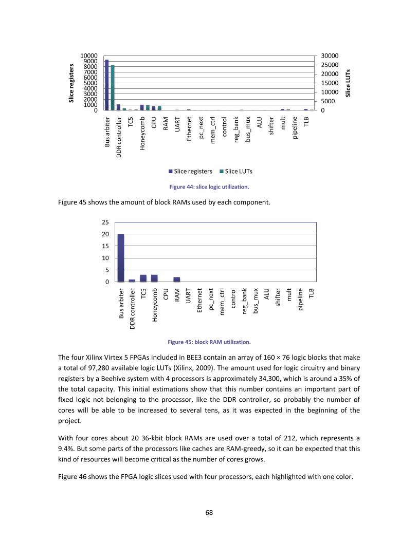
68
Figure 44: slice logic utilization.
Figure 45 shows the amount of block RAMs used by each component.
Figure 45: block RAM utilization.
The four Xilinx Virtex 5 FPGAs included in BEE3 contain an array of 160 × 76 logic blocks that make
a total of 97,280 available logic LUTs (Xilinx, 2009). The amount used for logic circuitry and binary
registers by a Beehive system with 4 processors is approximately 34,300, which is around a 35% of
the total capacity. This initial estimations show that this number contains an important part of
fixed logic not belonging to the processor, like the DDR controller, so probably the number of
cores will be able to be increased to several tens, as it was expected in the beginning of the
project.
With four cores about 20 36-kbit block RAMs are used over a total of 212, which represents a
9.4%. But some parts of the processors like caches are RAM-greedy, so it can be expected that this
kind of resources will become critical as the number of cores grows.
Figure 46 shows the FPGA logic slices used with four processors, each highlighted with one color.
0
5000
10000
15000
20000
25000
30000
0100020003000400050006000700080009000
10000
Bu
s ar
bit
er
DD
R c
on
tro
ller
TC5
Ho
ney
com
b
CP
U
RA
M
UA
RT
Eth
ern
et
pc_
nex
t
mem
_ctr
l
con
tro
l
reg_
ban
k
bu
s_m
ux
ALU
shif
ter
mu
lt
pip
elin
e
TLB
Slic
e LU
Ts
Slic
e r
egi
ste
rs
Slice registers Slice LUTs
0
5
10
15
20
25
Bu
s ar
bit
er
DD
R c
on
tro
ller
TC5
Ho
ney
com
b
CP
U
RA
M
UA
RT
Eth
ern
et
pc_
nex
t
mem
_ctr
l
con
tro
l
reg_
ban
k
bu
s_m
ux
ALU
shif
ter
mu
lt
pip
elin
e
TLB
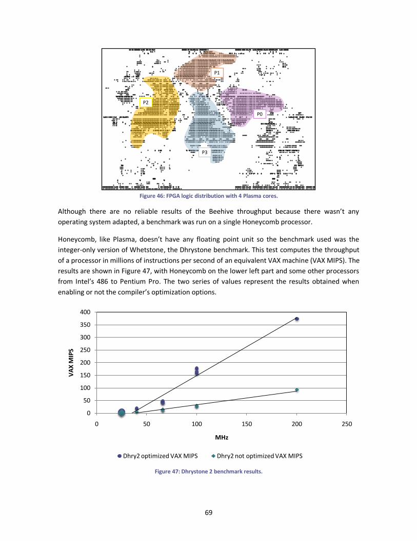
69
Figure 46: FPGA logic distribution with 4 Plasma cores.
Although there are no reliable results of the Beehive throughput because there wasn’t any
operating system adapted, a benchmark was run on a single Honeycomb processor.
Honeycomb, like Plasma, doesn’t have any floating point unit so the benchmark used was the
integer-only version of Whetstone, the Dhrystone benchmark. This test computes the throughput
of a processor in millions of instructions per second of an equivalent VAX machine (VAX MIPS). The
results are shown in Figure 47, with Honeycomb on the lower left part and some other processors
from Intel’s 486 to Pentium Pro. The two series of values represent the results obtained when
enabling or not the compiler’s optimization options.
Figure 47: Dhrystone 2 benchmark results.
0
50
100
150
200
250
300
350
400
0 50 100 150 200 250
VA
X M
IPS
MHz
Dhry2 optimized VAX MIPS Dhry2 not optimized VAX MIPS
P2
P1
P0
P3
70
It is clear the correlation between the processor speed and the result in the test. Honeycomb runs
at 25 MHz, a frequency considerably slower than other compared processors. Although its mark is
not bad, the fact that this processor has a cache of only 4 KB, while other processors have more
than 128 KB, can distort the results.
7.2 Future work This project will be continued at the BSC during the following months. In this section some
extensions and improvements of the current system are proposed and discussed.
Extend the Honeycomb pipeline. The current pipeline is the main limitation of the
processor’s speed. Refining the current stages would allow greater performance.
Modify the L1 cache to allow 16-byte refillings. The current DDR system works with lines
of 16 bytes, while the Honeycomb L1 cache can manage only 4 bytes. Adapting it to accept
lines of 16 bytes from the memory will save some cycles and reduce contention at the bus.
Develop hardware support for transactional memory. The original application of this
system.
Develop a minimal operating system for the platform. Currently a minimal operating
system called RTOS specially created for Plasma is being modified so it can handle virtual
memory and more than one processor.
Modify the bus arbiter to make use of the two DDR channels present in the FPGA. Each
BEE3 FPGA has two DDR modules, but for now only one is used. It could be possible to
replicate the current Beehive system to have two independent buses in each FPGA.
Extend the design to make use of the four FPGAs of the BEE3. This requires adding
hardware and system support for the BEE3 ring interconnection bus, which can be used
for message-passing and memory coherency.
Research and implement new CMP and MCMP coherency protocols. For example, token
coherency (Marty, et al., 2005) seems to be more efficient than traditional bus or directory
protocols on chip-multiprocessor (CMP) or multiple CMP (MCMP) systems.
Include coherency hardware support through LL/SC mechanisms.
7.3 Personal balance The beauty of this project resides in that it brings the opportunity to develop your own computer,
including processor, memory system, I/O controllers, operating system and new and exciting
features like transactional memory or token coherency mechanisms. This internship has been a
motivating challenge and a very reach experience. I’ve learned from scratch the fundamentals of
FPGA-based hardware design, and the work done from basic logic gates level to operating system
development and user-level software programming has given me a more deep comprehension
about the relation between hardware and software.
And finally, another interesting point about working at BSC has been the close contact with the
cutting-edge computer architecture researchers from this center or from other universities.
71
8 References
A Bluespec Implementation of an FPGA-based Photoshop Plug-In. Singh, Satnam. 2009. York,
United Kingdom : s.n., 2009. European Joint Conferences on Theory and Practice of Software.
A Cryptographic Coarse Grain Reconfigurable Architecture Robust Against DPA. Mesquita, Daniel,
et al. 2007. Long Beach, California, USA : IEEE International, 2007. Parallel and Distributed
Processing Symposium. pp. 1-8.
A Flexible Architecture for Simulation and Testing (FAST) Multiprocessor Systems. Davis, John D.,
Hammond, Lance and Olukotun, Kunle. 2005. s.l. : IEEE Computer Society, 2005. International
Symposium on High-Performance Computer Architecture.
A Logic Level Design Methodology for a Secure DPA Resistant ASIC or FPGA Implementation. Tiri,
Kris and Verbauwhede, Ingrid. 2004. Washington, DC : IEEE Computer Society, 2004. Proceedings
of the conference on Design, automation and test in Europe. Vol. 1.
BEE2: A High-End Reconfigurable Computing System. Chang, Chen, Wawrzynek, John and
Brodersen, Robert W. 2005. 2, s.l. : IEEE Computer Society, March 2005, IEEE Design and Test of
Computers, Vol. 22, pp. 114-125.
Cosoroaba, Adrian and Rivoallon, Frédéric. 2006. Achieving Higher System Performance with the
Virtex-5 Family of FPGAs. [White paper] s.l. : Xilinx Inc., 2006.
Davis, John D., Thacker, Charles P. and Chang, Chen. 2009. BEE3: Revitalizing Computer
Architecture Research. s.l. : Microsoft Research, 2009.
Design Automation Technical Committee of the IEEE Computer Society. 1993. IEEE standard
multivalue logic system for VHDL modelinteroperability (Std_logic_1164). s.l. : IEEE Computer
Society, 1993.
Experience Using a Low-Cost FPGA Design to Crack DES Keys. Clayton, Richard and Bond, Mike.
2003. Berlin : Springer, 2003. Cryptographic Hardware and Embedded Systems (CHES 2002). pp.
877-883.
72
Hansen, Craig C. and Riordan, Thomas J. 1989. RISC computer with unaligned reference handling
and method for the same. 4814976 USA, March 21, 1989. Hardware patent.
Hauck, Scott and Dehon, André. 2008. Reconfigurable computing. Burlington, Massachusetts,
USA : Morgan Kauffman, 2008.
Implementation of BEE: a Real-time Large-scale Hardware Emulation Engine. Chang, Chen, et al.
2003. Monterey, California : ACM, 2003. Proceedings of the FPGA conference. pp. 91-99.
Improving Multiple-CMP Systems Using Token Coherence. Marty, Michael R., et al. 2005. s.l. : IEEE,
2005. Proceedings of the 11th International Symposium on High-Performance Computer
Architecture.
Kane, Gerry and Heinrich, Joe. 1992. MIPS RISC architecture. New Jersey : Prentice Hall PTR, 1992.
Larrabee: A Many-Core x86 Architecture for Visual Computing. Seiler, Larry, et al. 2008. 3, s.l. :
ACM, August 2008, ACM Transactions on Graphics, Vol. 27.
Limits to binary logic switch scaling - a gedanken model. Zhirnov, Victor V., et al. 2003. 11, s.l. :
IEEE, 2003, Proceedings of the IEEE, Vol. 91, pp. 1934-1939.
MIPS RISC Architecture. Mashley, John. 1989. Palo Alto, California : IEEE, 1989. Proceedings of the
HOT CHIPS 1 Symposium on High-Performance Chips.
MIPS Technologies, Inc. 2009. MIPS32 Architecture For Programmers. 2009. Vol. II: The MIPS32
Instruction Set.
RAMP Blue: Implementation of a Manycore 1008 Processor FPGA System. Burke, D., et al. 2008.
Urbana, Illinois : s.n., 2008. Proceedings of the Reconfigurable Systems Summer Institute.
Rapid Prototyping for DSP Systems with Multiprocessors. Engels, Marc, Lauwereins, Rudy and
Peperstraete, J.A. 1991. 2, s.l. : IEEE Computer Society, 1991, IEEE Design and Test of Computers,
Vol. 8, pp. 52-62.
Rhoads, Steve. 2001. Plasma - most MIPS I (TM) opcodes. Opencores. [Online] 2001.
http://www.opencores.org/project,plasma.
Skowronek, Stanislaw. 2007. NSA@home: a fast FPGA-based SHA1 and MD5 bruteforce cracker.
Unaligned.org. [Online] 2007. http://nsa.unaligned.org.
Sweetman, Dominic. 2007. See MIPS run. San Francisco : Morgan Kaufmann Publishers / Elsevier,
2007.
Thacker, Chuck. 2009. A DDR2 Controller for BEE3. s.l. : Microsoft Research, 2009.
Turbocharging Your CPU with an FPGA-Programmable Coprocessor. O'Rourke, Barry and Taylor,
Richard. 2006. 58, s.l. : Xillinx, Inc., 2006, XCell, pp. 52-54.
73
University of California. 2009. Research Accelerator for Multiple Processors. [Online] 2009.
http://ramp.eecs.berkeley.edu/.
Wakerly, John F. 2006. Digital Design: principles and practices. Fourth Edition. Upper Saddle River,
New Jersey, USA : Pearson Prentice Hall, 2006.
Will physical scalability sabotage performance gains? Matzke, Doug. 1997. 9, s.l. : IEEE, September
1997, Computer, Vol. 30, pp. 37-39.
Xilinx. 2009. DS100: Virtex-5 Family Overview. Xilinx. [Online] Xilinx Inc., February 2009.
http://www.xilinx.com/support/documentation/data_sheets/ds100.pdf.
—. 2008. DS253: Content-Addressable Memory v6.1. Xilinx. [Online] September 19, 2008.
http://www.xilinx.com/support/documentation/ip_documentation/cam_ds253.pdf.
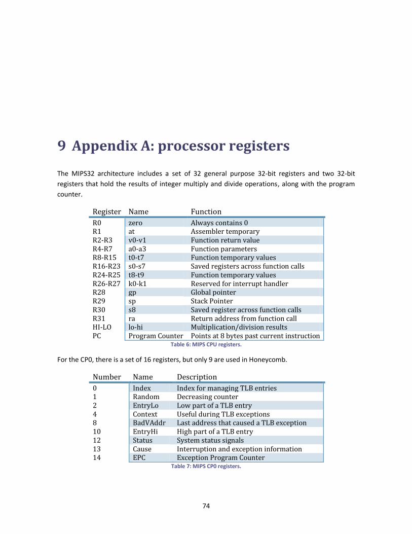
74
9 Appendix A: processor registers
The MIPS32 architecture includes a set of 32 general purpose 32-bit registers and two 32-bit
registers that hold the results of integer multiply and divide operations, along with the program
counter.
Register Name Function
R0 zero Always contains 0 R1 at Assembler temporary R2-R3 v0-v1 Function return value R4-R7 a0-a3 Function parameters R8-R15 t0-t7 Function temporary values R16-R23 s0-s7 Saved registers across function calls R24-R25 t8-t9 Function temporary values R26-R27 k0-k1 Reserved for interrupt handler R28 gp Global pointer R29 sp Stack Pointer R30 s8 Saved register across function calls R31 ra Return address from function call HI-LO lo-hi Multiplication/division results PC Program Counter Points at 8 bytes past current instruction
Table 6: MIPS CPU registers.
For the CP0, there is a set of 16 registers, but only 9 are used in Honeycomb.
Number Name Description
0 Index Index for managing TLB entries 1 Random Decreasing counter 2 EntryLo Low part of a TLB entry 4 Context Useful during TLB exceptions 8 BadVAddr Last address that caused a TLB exception 10 EntryHi High part of a TLB entry 12 Status System status signals 13 Cause Interruption and exception information 14 EPC Exception Program Counter
Table 7: MIPS CP0 registers.
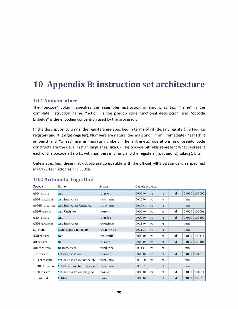
75
10 Appendix B: instruction set architecture
10.1 Nomenclature The “opcode” column specifies the assembler instruction mnemonic syntax; “name” is the
complete instruction name; “action” is the pseudo code functional description; and “opcode
bitfields” is the encoding convention used by the processor.
In the description columns, the registers are specified in terms of rd (destiny register), rs (source
register) and rt (target register). Numbers are natural decimals and “imm” (immediate), “sa” (shift
amount) and “offset” are immediate numbers. The arithmetic operations and pseudo code
constructs are the usual in high languages (like C). The opcode bitfields represent what represent
each of the opcode’s 32 bits, with numbers in binary and the registers (rs, rt and rd) taking 5 bits.
Unless specified, these instructions are compatible with the official MIPS 32 standard as specified
in (MIPS Technologies, Inc., 2009).
10.2 Arithmetic Logic Unit Opcode Name Action Opcode bitfields
ADD rd,rs,rt Add rd=rs+rt 000000 rs rt rd 00000 100000
ADDI rt,rs,imm Add Immediate rt=rs+imm 001000 rs rt imm
ADDIU rt,rs,imm Add Immediate Unsigned rt=rs+imm 001001 rs rt imm
ADDU rd,rs,rt Add Unsigned rd=rs+rt 000000 rs rt rd 00000 100001
AND rd,rs,rt And rd=rs&rt 000000 rs rt rd 00000 100100
ANDI rt,rs,imm And Immediate rt=rs&imm 001100 rs rt imm
LUI rt,imm Load Upper Immediate rt=imm<<16 001111 rs rt imm
NOR rd,rs,rt Nor rd=~(rs|rt) 000000 rs rt rd 00000 100111
OR rd,rs,rt Or rd=rs|rt 000000 rs rt rd 00000 100101
ORI rt,rs,imm Or Immediate rt=rs|imm 001101 rs rt imm
SLT rd,rs,rt Set On Less Than rd=rs<rt 000000 rs rt rd 00000 101010
SLTI rt,rs,imm Set On Less Than Immediate rt=rs<imm 001010 rs rt imm
SLTIU rt,rs,imm Set On < Immediate Unsigned rt=rs<imm 001011 rs rt imm
SLTU rd,rs,rt Set On Less Than Unsigned rd=rs<rt 000000 rs rt rd 00000 101011
SUB rd,rs,rt Subtract rd=rs-rt 000000 rs rt rd 00000 100010
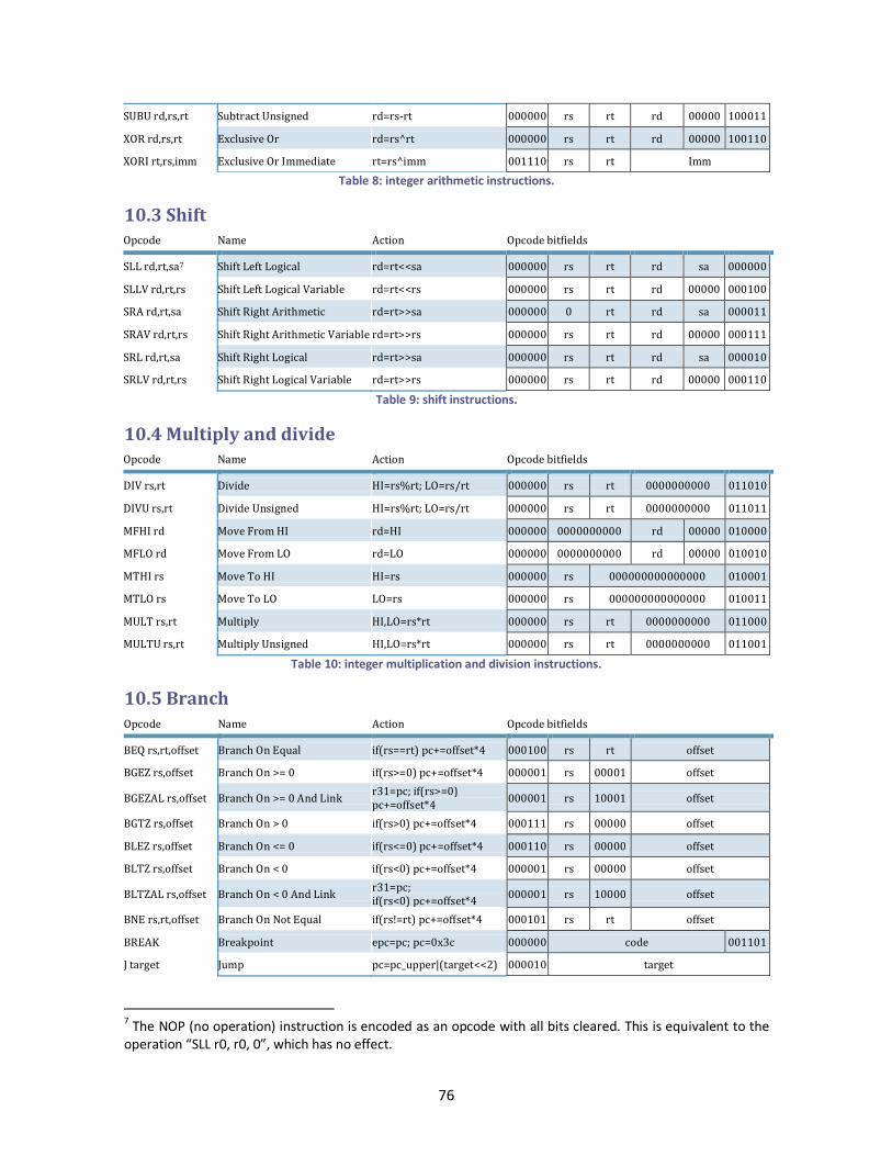
76
SUBU rd,rs,rt Subtract Unsigned rd=rs-rt 000000 rs rt rd 00000 100011
XOR rd,rs,rt Exclusive Or rd=rs^rt 000000 rs rt rd 00000 100110
XORI rt,rs,imm Exclusive Or Immediate rt=rs^imm 001110 rs rt Imm
Table 8: integer arithmetic instructions.
10.3 Shift Opcode Name Action Opcode bitfields
SLL rd,rt,sa7 Shift Left Logical rd=rt<<sa 000000 rs rt rd sa 000000
SLLV rd,rt,rs Shift Left Logical Variable rd=rt<<rs 000000 rs rt rd 00000 000100
SRA rd,rt,sa Shift Right Arithmetic rd=rt>>sa 000000 0 rt rd sa 000011
SRAV rd,rt,rs Shift Right Arithmetic Variable rd=rt>>rs 000000 rs rt rd 00000 000111
SRL rd,rt,sa Shift Right Logical rd=rt>>sa 000000 rs rt rd sa 000010
SRLV rd,rt,rs Shift Right Logical Variable rd=rt>>rs 000000 rs rt rd 00000 000110
Table 9: shift instructions.
10.4 Multiply and divide Opcode Name Action Opcode bitfields
DIV rs,rt Divide HI=rs%rt; LO=rs/rt 000000 rs rt 0000000000 011010
DIVU rs,rt Divide Unsigned HI=rs%rt; LO=rs/rt 000000 rs rt 0000000000 011011
MFHI rd Move From HI rd=HI 000000 0000000000 rd 00000 010000
MFLO rd Move From LO rd=LO 000000 0000000000 rd 00000 010010
MTHI rs Move To HI HI=rs 000000 rs 000000000000000 010001
MTLO rs Move To LO LO=rs 000000 rs 000000000000000 010011
MULT rs,rt Multiply HI,LO=rs*rt 000000 rs rt 0000000000 011000
MULTU rs,rt Multiply Unsigned HI,LO=rs*rt 000000 rs rt 0000000000 011001
Table 10: integer multiplication and division instructions.
10.5 Branch Opcode Name Action Opcode bitfields
BEQ rs,rt,offset Branch On Equal if(rs==rt) pc+=offset*4 000100 rs rt offset
BGEZ rs,offset Branch On >= 0 if(rs>=0) pc+=offset*4 000001 rs 00001 offset
BGEZAL rs,offset Branch On >= 0 And Link r31=pc; if(rs>=0) pc+=offset*4
000001 rs 10001 offset
BGTZ rs,offset Branch On > 0 if(rs>0) pc+=offset*4 000111 rs 00000 offset
BLEZ rs,offset Branch On <= 0 if(rs<=0) pc+=offset*4 000110 rs 00000 offset
BLTZ rs,offset Branch On < 0 if(rs<0) pc+=offset*4 000001 rs 00000 offset
BLTZAL rs,offset Branch On < 0 And Link r31=pc; if(rs<0) pc+=offset*4
000001 rs 10000 offset
BNE rs,rt,offset Branch On Not Equal if(rs!=rt) pc+=offset*4 000101 rs rt offset
BREAK Breakpoint epc=pc; pc=0x3c 000000 code 001101
J target Jump pc=pc_upper|(target<<2) 000010 target
7 The NOP (no operation) instruction is encoded as an opcode with all bits cleared. This is equivalent to the operation “SLL r0, r0, 0”, which has no effect.
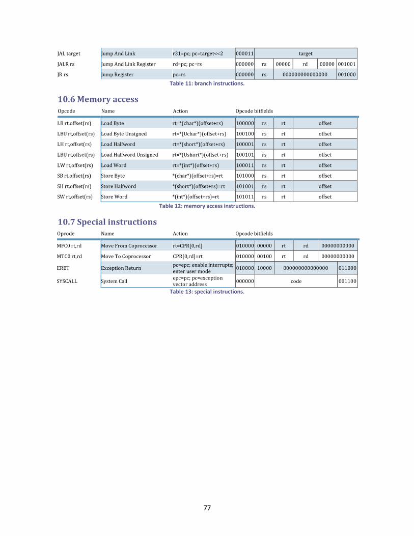
77
JAL target Jump And Link r31=pc; pc=target<<2 000011 target
JALR rs Jump And Link Register rd=pc; pc=rs 000000 rs 00000 rd 00000 001001
JR rs Jump Register pc=rs 000000 rs 000000000000000 001000
Table 11: branch instructions.
10.6 Memory access Opcode Name Action Opcode bitfields
LB rt,offset(rs) Load Byte rt=*(char*)(offset+rs) 100000 rs rt offset
LBU rt,offset(rs) Load Byte Unsigned rt=*(Uchar*)(offset+rs) 100100 rs rt offset
LH rt,offset(rs) Load Halfword rt=*(short*)(offset+rs) 100001 rs rt offset
LBU rt,offset(rs) Load Halfword Unsigned rt=*(Ushort*)(offset+rs) 100101 rs rt offset
LW rt,offset(rs) Load Word rt=*(int*)(offset+rs) 100011 rs rt offset
SB rt,offset(rs) Store Byte *(char*)(offset+rs)=rt 101000 rs rt offset
SH rt,offset(rs) Store Halfword *(short*)(offset+rs)=rt 101001 rs rt offset
SW rt,offset(rs) Store Word *(int*)(offset+rs)=rt 101011 rs rt offset
Table 12: memory access instructions.
10.7 Special instructions Opcode Name Action Opcode bitfields
MFC0 rt,rd Move From Coprocessor rt=CPR[0,rd] 010000 00000 rt rd 00000000000
MTC0 rt,rd Move To Coprocessor CPR[0,rd]=rt 010000 00100 rt rd 00000000000
ERET Exception Return pc=epc; enable interrupts; enter user mode
010000 10000 000000000000000 011000
SYSCALL System Call epc=pc; pc=exception vector address
000000 code 001100
Table 13: special instructions.