
Diseño de un BMS para un vehículo eléctrico
148
UNIVERSITAT POLITÈCNICA DE VALÈNCIA Escuela Técnica Superior de Ingeniería de Diseño TRABAJO FINAL DE GRADO Grado de Ingeniería eléctrica Diseño de un BMS para un vehículo eléctrico Autor: Alberto Castillo Ribelles Tutor: Francisco Rodríguez Benito Valencia, septiembre de 2019
Transcript of Diseño de un BMS para un vehículo eléctrico

UNIVERSITAT POLITÈCNICA DE VALÈNCIA
Escuela Técnica Superior de Ingeniería de Diseño
TRABAJO FINAL DE GRADO
Grado de Ingeniería eléctrica
Diseño de un BMS para un vehículo eléctrico
Autor: Alberto Castillo Ribelles
Tutor: Francisco Rodríguez Benito
Valencia, septiembre de 2019

Resumen
A lo largo del presente proyecto se explica la importancia de los Battery Management System
(BMS de aquí en adelante) en los sistemas de almacenamiento energético, así como su
funcionamiento, morfología y funciones. Por otro lado, se detalla el procedimiento seguido para
el diseño, construcción y desarrollo de un BMS propio basado en el microchip AD7280A de
Analog Devices. Además, se explican las diferentes mejoras que se pueden aplicar al prototipo
a fin de mejorar su escalabilidad, durabilidad y seguridad.

2
Índice
RESUMEN .......................................................................................................................................... 1
MOTIVACIÓN Y OBJETIVOS ................................................................................................................. 5
INTRODUCCIÓN .................................................................................................................................. 7
BATERÍAS DE LITIO ............................................................................................................................. 8
LITIO-IÓN .................................................................................................................................................... 8 LITIO FERROFOSFATO ..................................................................................................................................... 9 POLÍMERO DE LITIO...................................................................................................................................... 10 CARGA DEL LITIO ......................................................................................................................................... 11
BATTERY MANAGEMENT SYSTEM ...................................................................................................... 12
DEFINICIÓN ................................................................................................................................................ 12 BMS PARA BATERÍAS DE LITIO-IÓN ................................................................................................................. 12
Asociación serie-paralelo ................................................................................................................... 16 FUNCIONES ................................................................................................................................................ 18
Medición ............................................................................................................................................ 18 Gestión ............................................................................................................................................... 19 Evaluación .......................................................................................................................................... 20 Comunicación .................................................................................................................................... 21
TIPOLOGÍA ................................................................................................................................................. 21 Centralizado ....................................................................................................................................... 22 Modular ............................................................................................................................................. 22 Master-Slave ...................................................................................................................................... 23 Distribuido ......................................................................................................................................... 23 Comparación ...................................................................................................................................... 24
CONSTRUCCIÓN DE UN BMS .............................................................................................................. 25
TIPOLOGÍA Y BASE ELECTRÓNICA ..................................................................................................................... 25 DISEÑO DEL ESQUEMA ELÉCTRICO ................................................................................................................... 25 MATERIALES .............................................................................................................................................. 30 CONSTRUCCIÓN .......................................................................................................................................... 31 ERRORES Y SOLUCIONES ................................................................................................................................ 43 RESULTADOS .............................................................................................................................................. 46 MEJORA DEL SISTEMA .................................................................................................................................. 47 PRESUPUESTO ............................................................................................................................................ 48 COMPARACIÓN CON OTROS PRODUCTOS .......................................................................................................... 49
CONSTRUCCIÓN DE UN CARGADOR INTEGRADO EN EL BMS .............................................................. 51
PLANOS ............................................................................................................................................. 54
PLANO PLACA PCB MÁSTER .......................................................................................................................... 54 PLANO PLACA PCB SISTEMA DE BALANCEO SLAVES ............................................................................................. 54
BIBLIOGRAFÍA ................................................................................................................................... 55
DATASHEETS ..................................................................................................................................... 55

Diseño de un BMS para un vehículo eléctrico
Glosario de figuras
Figura 1. Gráfica de relación tensión-capacidad de una batería Samsung INR18650-30Q .......... 8
Figura 2. Gráfica de carga de una batería Samsung INR18650-30Q ........................................... 11
Figura 3. Cargador de litio para una batería. Esquema y modelo usado en los cargadores de
teléfonos móviles. ....................................................................................................................... 11
Figura 4. Cargador de litio para dos baterías en serie basado en la familia MCP de Microchip. 11
Figura 5. Grupo de baterías en serie: (a) desbalanceadas (b) balanceadas ................................ 12
Figura 6. Dos baterías en serie cargadas: (a) balanceadas (b) desbalanceadas .......................... 13
Figura 7. Pack de baterías en serie: (a) cargado balanceado; (b) cargado desbalanceado; (c)
descargado balanceado; (d) descargado desbalanceado ........................................................... 13
Figura 8. Pequeño grupo en serie de baja capacidad. (a) Al estar una de ellas desbalanceada con
el resto, el pack completo se ve afectado. (b) pack totalmente balanceado. ............................ 14
Figura 9. Pack de baterías ideal autodescargandose con el paso del tiempo ............................. 15
Figura 10. Pack de baterías real autodescargandose con el paso del tiempo ............................ 15
Figura 11. Tipos de asociación: (a) serie-paralelo; (b) paralelo-serie ......................................... 16
Figura 12. Celdas con una resistencia interna elevada provocan desbalanceo cuando los bloques
se asocian en paralelo (a), pero no cuando las celdas se asocian en paralelo (b) ...................... 16
Figura 13. Múltiples baterías de poca capacidad afectan más en bloques en serie (a) que con las
celdas en paralelo (b) .................................................................................................................. 17
Figura 14. La rotura de una celda destruye el bloque entero en el que esté situado (a), pero si
está en paralelo con otras celdas (b) no afecta al resto de baterías. ......................................... 17
Figura 15. Celdas directamente en paralelo (a) necesitan menos conexiones de BMS que hilos
en paralelo (b) ............................................................................................................................. 18
Figura 16. La apertura o rotura del shunt es transformada en una señal digital mediante el
amplificador y mandada al BMS .................................................................................................. 19
Figura 17. Tipos de balanceo: (a) pasivo y (b) activo .................................................................. 20
Figura 18. Se puede captar la temperatura por celda (a) o por pack completo (b) .................... 20
Figura 19. BMS centralizado ........................................................................................................ 22
Figura 20. BMS modular .............................................................................................................. 22
Figura 21. BMS master-slave ....................................................................................................... 23
Figura 22. BMS distribuido .......................................................................................................... 24
Figura 23. Tamaño en mm del formato LQFP48 ......................................................................... 25
Figura 24. Diagrama de configuración para 6 celdas .................................................................. 26
Figura 25. Diagrama de configuración de los termistores en A7280A ........................................ 26
Figura 26. Diagrama de configuración modular para más de 6 celdas ....................................... 27
Figura 27. Esquema simplificado del montaje de una asociación en serie de seis baterías ....... 28
Figura 28. Representación de la apertura del MOSFET y la disipación de la energía de la batería.
..................................................................................................................................................... 28
Figura 29. Región ohmica del 2N7000G. En rojo la posición en la que se encontraría en nuestro
circuito. ........................................................................................................................................ 29
Figura 30. Esquema de la simulación en LTspice XVII ................................................................. 29
Figura 31. Esquema de la apertura del MOSFET que controla el balanceo de la tercera batería.
..................................................................................................................................................... 30
Figura 32. Representación del valor de la intensidad que pasa a través de cada resistencia de
balanceo, siendo en verde la intensidad que pasa a través de la tercera resistencia, mientras que
las otras son el resto de colores. ................................................................................................. 30

Diseño de un BMS para un vehículo eléctrico
4
Figura 33. Paquete de protección externo del microchip AD7280A ........................................... 32
Figura 34. Caja de protección en donde se encuentran los microchips ..................................... 32
Figura 35. Protección acolchada interna en donde se encuentran los microchips .................... 32
Figura 36. Tamaño real del microchip AD7280A frente a una regla ........................................... 33
Figura 37. Adaptador de LQFP48 a pin estándar ........................................................................ 33
Figura 38. Adaptador y microchip soldados ................................................................................ 33
Figura 39. Los tres procesadores soldados a sus adaptadores ................................................... 33
Figura 40. Parte trasera de la PCB con los pines de los adaptadores soldados .......................... 34
Figura 41. Parte delantera de la PCB con los adaptadores soldados y a la izquierda los terminales
de conexión al microprocesador (Arduino) ................................................................................ 34
Figura 42. Parte trasera de la PCB con la conexión del microchip (máster) a los terminales de
conexión al microprocesador ...................................................................................................... 34
Figura 43. Primeras conexiones a la Daisy Chain (cableado verde) ............................................ 35
Figura 44. Primera Daisy Chain soldada y elementos auxiliares del microchip master. ............. 35
Figura 45. Todos los elementos electrónicos auxiliares, zona de balanceo pasivo (parte superior
de la PCB) y Daisy Chain del primer microchip soldados ............................................................ 35
Figura 46. Conexiones traseras mediante cableado del microchip máster, y Daisy Chain entre
éste y el segundo microchip ........................................................................................................ 36
Figura 47. Imagen en detalle de la Daisy Chain (cableado verde y rojo) .................................... 36
Figura 48. Comienzo de conexión del segundo microchip .......................................................... 36
Figura 49. Cableado y elementos externos soldados de todos los microchips excepto por las
conexiones a las áreas de balanceo ............................................................................................ 37
Figura 50. Parte superior de la PCB junto con seis adaptadores de baterías ............................. 37
Figura 51. Baterías Samsung ICR18650-26J ................................................................................ 38
Figura 52. Prueba de funcionamiento del microchip .................................................................. 38
Figura 53. Módulo final, con iluminación LED en paralelo a cada resistencia ............................ 39
Figura 54. Ensamblaje del circuito de balanceo pasivo del primer slave. ................................... 39
Figura 55. Circuitos de balanceo del primer y segundo slave, para seis y cuatro bloques
respectivamente. ........................................................................................................................ 40
Figura 56. Unión de ambas placas PCB. ...................................................................................... 40
Figura 57. Ensamblaje de las conexiones del circuito pasivo del primer slave al microchip. ..... 40
Figura 58. Todas las conexiones realizadas del sistema BMS. .................................................... 41
Figura 59. Unión de 16 bases para baterías con formato 18650. ............................................... 41
Figura 60. 16 baterías Samsung ICR18650-26J ............................................................................ 42
Figura 61. Medición de tensión en bornes del pack de baterías. 62,5 V .................................... 42
Figura 62. Conexión de las baterías con el BMS. ......................................................................... 42
Figura 63. Situación del fallo de soldadura ................................................................................. 43
Figura 64. Valores de tensiones obtenidos ................................................................................. 44
Figura 65. Valores de tensión obtenidos en todo el sistema de balanceo. ................................ 44
Figura 66. Modelo MCP7 frente a una regla de medir en cm. Se comprueba que sus lados miden
3mm. ........................................................................................................................................... 51
Figura 67. A la izquierda el microchip ya soldado; a la derecha el propio adaptador. ............... 51
Figura 68. Esquema eléctrico de un microchip de carga. ........................................................... 51
Figura 69. Comprobación del funcionamiento del chip. A la izquierda las baterías cargándose, y
a la derecha una batería junto a un boost haciendo de fuente de alimentación para el chip. .. 52
Figura 70. Comprobación de funcionamiento de un chip soldado a la placa PCB. ..................... 52
Figura 71. Sistema (a) sin separación de circuitos. Sistema (b) con circuitos separados. .......... 53

Diseño de un BMS para un vehículo eléctrico
5
Glosario de tablas Tabla 1. Especificaciones del ión-litio ............................................................................................ 9
Tabla 2. Ventajas y desventajas de ión-litio .................................................................................. 9
Tabla 3. Especificaciones del litio ferrofosfato. ............................................................................ 9
Tabla 4. Ventjas y desventajas de litio-ferrofosfato ................................................................... 10
Tabla 5. Especificaciones del Polímero de litio. .......................................................................... 10
Tabla 6. Ventajas y desventajas de Polímero de litio. ................................................................. 10
Tabla 7. Comparación de las distintas tipologias de BMS. .......................................................... 24
Tabla 8. Lista de componentes electrónicos para la construcción del BMS ............................... 31
Tabla 9. Valores de los parámetros del máster. .......................................................................... 47
Tabla 10. Valores de los parámetros del slave 1. ........................................................................ 47
Tabla 11. Valores de los parámetros del slave 2. ........................................................................ 47
Tabla 12. Coste de los componentes para la construcción del BMS. .......................................... 48
Tabla 13. Coste de los componentes para la construcción del pack de baterías. ....................... 49
Tabla 14. División del tiempo de trabajo. ................................................................................... 49
Tabla 15. Coste total del proyecto. ............................................................................................. 49
Tabla 16. Listado de otros sistemas BMS en comparación con el nuestro. ................................ 50

Diseño de un BMS para un vehículo eléctrico
6
Motivación y objetivos
El objetivo del presente trabajo de fin de grado es el diseño y construcción de un Battery
Management System, totalmente escalable a cualquier configuración serie-paralelo de baterías
de dicha tecnología y adaptable a cualquier finalidad o requerimiento del sistema. Además, se
tendrá en cuenta que el sistema diseñado sea barato, sencillo, de fácil construcción, de fácil
comprensión, y plug and play.
La idea de que el presente proyecto tratase sobre dicho elemento de control y carga se debe a
que en los últimos años de mi vida académica y profesional he estado presente en diferentes
proyectos, cuyo objetivo era la creación de un vehículo híbrido de competición, un vehículo
eléctrico o una estación de recarga para estos vehículos. El elemento común que une estos
proyectos, y del que me encargaba, son las baterías, su sistema de control BMS y la carga de las
propias baterías.

Diseño de un BMS para un vehículo eléctrico
7
Introducción
Con el creciente aumento del uso de baterías de litio, tales como el litio-ión o el Polímero de litio
en coches eléctricos, estaciones de almacenamiento energéticos, pequeños vehículos de
movilidad eléctrica, smartphones u ordenadores portátiles, ha crecido la demanda de elementos
que sean capaces de controlar y garantizar la seguridad de las baterías. Para estas labores se
diseñaron los Battery Management System (BMS), que son sistemas electrónicos complejos que
se conectan directamente al pack de baterías, monitorizándolo y protegiéndolo. Debido a la
naturaleza de las baterías estos sistemas son necesarios en la inmensa mayoría de casos, por lo
que su demanda sigue a la de las propias baterías.
Gracias a estos últimos, el mercado de BMS ha crecido exponencialmente estos años,
permitiendo abaratar estos dispositivos electrónicos de control y seguridad para las baterías de
litio. No obstante, los sistemas que se comercializan tienen poca intensidad de descarga y
admiten poca tensión en bornes, haciendo imposible poder utilizar dichos BMS en sistemas de
mayor potencia, tales como vehículos eléctricos o almacenamiento energético. Para estos
sistemas existen compañías que crean BMS específicos para las necesidades del cliente, pero si
este sistema de control y protección ha de ser flexible en sus parámetros se debe diseñar y crear
un BMS completamente. De aquí nace el objetivo del presente Trabajo de Fin de Grado.
Este tipo de electrónica de control es relativamente nueva, pues tuvo que nacer a la vez que las
baterías de litio-ión salían al mercado a principios de los años 90. Debido a ello existe muy pocos
especialistas en la materia, pocos libros con información detallada, y en algunos casos la
información encontrada puede diferir bastante entre autores.

Diseño de un BMS para un vehículo eléctrico
8
Baterías de litio
Antes de comenzar la explicación sobre los Battery Management System, es necesario conocer
la naturaleza de las baterías de litio, que es la que las hace dependiente de estos sistemas de
protección.
Litio-ión
El litio, con todas sus vertientes tecnológicas, ha hecho evolucionar en diez años al sector del
almacenamiento energético todo lo que a mediados de siglo XX se prometió con el níquel. Las
características técnicas que esta tecnología ofrece no se pueden comparar con ninguna otra en
el mercado, pues llegan a doblar la energía específica de las baterías de NIMH, triplicar la
densidad energética y son capaces de proporcionar un pico de potencia que solo es superado
por las baterías de Polímero de litio. Esta tecnología nos ha permitido desarrollar teléfonos
móviles con baterías suficientemente energéticas, se han desarrollado y comercializado
vehículos eléctricos e híbridos con una autonomía que cada año se supera, y se han creado
centros de almacenamiento energético a pequeña y gran escala.
Uno de los principales inconvenientes que estas tienen es la diferencia de tensión que
proporcionan entre la carga máxima (4.2V) y su carga mínima (3-2.5 V) (Figura 1). Aunque con
una batería no resulte una gran diferencia, cuando estas se en serializan el problema aumenta
llegando a existir una diferencia de 140V por cada 100 serie de baterías. Esto repercute en la
necesidad de incluir un convertidor DC-DC a la salida de cada pack, y por tanto un significativo
aumento del coste.
Figura 1. Gráfica de relación tensión-capacidad de una batería Samsung INR18650-30Q
Otro de los problemas que esta tecnología presenta es la seguridad tanto de ella como de su
entorno. La rápida degradación con el paso del tiempo y el peligro que encarna esta tecnología
frente a los entornos no controlados, la hacen dependiente de sistemas electrónicos que las
controlen y mantengan fuera de todo peligro. Pese a los dispositivos de seguridad adicionales
que se instalan, están baterías pueden inflamarse rápidamente en caso de golpe o destrucción
parcial de su carcasa.
Por otro lado, se encuentra en contante desarrollo la carga rápida de esta tecnología, que es una
de las grandes objeciones del consumidor. En un principio, estas baterías solo podían cargarse a
4,2
4,1
4,0
3,9
3,8
3,7
3,6
3,5
3,4
3,3
3,2
3,1
3,0
2,9
2,8
0,25 0,50 0,75 1,251,00 1,50 1,75 2,00 3,002,25 2,50 2,75 3,25
Vo
lta
je (
V)
Capacidad (Ah)

Diseño de un BMS para un vehículo eléctrico
9
0,1C1 o existía riesgo de explosión y sobrecarga. En esta última media década se han conseguido
cargas totalmente seguras a 4C, posibilitando cargar los grandes sistemas de almacenamiento,
como los vehículos eléctricos, de manera rápida.
Existen diferentes combinaciones electroquímicas para las baterías de litio, dando lugar a las
baterías de polímero de litio-ión (LiPo), fosfato de hierro de litio (LiFePo4), y de estado sólido
entre otras.
Tabla 1. Especificaciones del ión-litio
Ventajas Desventajas
Alta densidad energética
Enorme potencia eléctrica
Número de ciclos alto
Degradación con el tiempo
Peligrosa si no se trata adecuadamente
Difícil extinción en caso de incendio
Requiere personal cualificado para su manejo
Tensión variable
Tabla 2. Ventajas y desventajas de ión-litio
Litio ferrofosfato
Una de las variantes más utilizadas del ión-litio son las baterías de litio-ferrofosfato,
abreviadamente dicho LiFePo4 o LFP, debido a su seguridad, durabilidad, coste y baja toxicidad.
El nombre de esta tecnología viene por la composición empleada, pues utiliza un elemento de
la familia del hierro como cátodo, y solucionando su baja conductividad empleando metales
conductores como dopantes.
El LFP, al ser de la misma familia que el ión-litio, tiene muchas características comunes a éste,
sin embargo, existen varias diferencias. La primera de ellas, y la más reseñable, es el cambio de
tensiones tanto nominales y máximas. El gráfico de tensiones de esta tecnología es mucho más
plano y constante en el rango entre 3,3 a 3 voltios. Además, tienen menores características
eléctricas que el ión-litio, tanto por peso, volumen y potencia.
Tabla 3. Especificaciones del litio ferrofosfato.
1 El significado de XC es la cantidad de amperaje que proporciona o recibe la batería. Este número se calcula dividiendo el amperaje por los amperios hora nominales de la batería. Es decir, si una batería descarga a 2C, y posee 2200mAh, significa que está descargando 4.4 amperios.
Ión-litio
Tensión nominal (V)
Tensión máxima (V)
Tensión mínima (V)
Energía específica (Wh/Kg)
Densidad energética (Wh/l)
Potencia/peso (W/Kg)
3,6 4,2 2,5 150-280 200-760 160-2800
Litio ferrofosfato
Tensión nominal (V)
Tensión máxima (V)
Tensión mínima (V)
Energía específica (Wh/Kg)
Densidad energética (Wh/l)
Potencia/peso (W/Kg)
3,2 3,65 2,5 100 180-240 350

Diseño de un BMS para un vehículo eléctrico
10
Tabla 4. Ventajas y desventajas de litio-ferrofosfato
Polímero de litio
Las baterías de polímero de litio-ión, abreviadamente LiPo, son baterías recargables que utilizan
el mismo proceso químico que las baterías de ión-litio, aunque en vez de emplear un electrolito
líquido emplean un polímero gelificado. Posen casi las mismas características eléctricas que las
baterías de litio-ión, aunque su principal diferencia es que éstas pueden llegar a descargar hasta
a 150C durante un periodo de tiempo de 10 segundos, mientras que en ese periodo de tiempo
las de ión solamente llegan a 10C. Estas potentes descargas afectan seriamente a la vida útil de
la tecnología, por lo que no es nada recomendable para usos con grandes ciclos de carga y
descarga.
Respecto a la seguridad y utilización de estas baterías, cabe destacar que son un poco más
peligrosas que la tecnología de ión-litio, por lo que la hace más delicadas tanto en el transporte
como en su utilización.
Existe una variante en el mercado que utiliza grafeno como elemento para el proceso químico,
haciendo que la relación potencia peso aumente considerablemente. Esta tecnología es capaz
de llegar fácilmente a picos de 200C, descargar constantemente a 90C y tener cargas rápidas a
5C sin peligro de dañar la batería.
Tabla 5. Especificaciones del Polímero de litio.
Ventajas Desventajas
Alta densidad energética
Máxima potencia eléctrica
Tensión por celda (3,6)
Degradación con el tiempo
Peligrosa si no se trata adecuadamente
Difícil extinción en caso de incendio
Requiere personal cualificado para su manejo
Problemas con el transporte internacional
Tensión variable
Precio
Tabla 6. Ventajas y desventajas de Polímero de litio.
Ventajas Desventajas
Seguridad
Parámetros eléctricos aceptables
Tensión casi estable
Parámetros eléctricos inferiores al litio-ión.
Mismas desventajas que el ión-litio
Polímero de litio
Tensión nominal (V)
Tensión máxima (V)
Tensión mínima (V)
Energía específica (Wh/Kg)
Densidad energética
(Wh/l)
Potencia/peso (W/Kg)
3,6 4,2 2,8 100-270 200-730 1500-4000

Diseño de un BMS para un vehículo eléctrico
11
Carga del litio
La carga de todas las baterías cuya tecnología se basa en el litio siguen el mismo régimen llamado
CC/CV. El significado de estas siglas es Constant Current/Constant Voltage, lo que traducido es
Corriente Constante/Tensión Constante. Este régimen está visualmente explicado en la Figura 2
Figura 2. Gráfica de carga de una batería Samsung INR18650-30Q
La empresa responsable de cada batería especifica el valor de la intensidad de carga (Ic) y de la
tensión máxima y mínima de la batería. Se deben seguir esos límites de tensión establecidos
para que la batería no sufra ningún daño. Sin embargo, la intensidad de carga que establece el
fabricante puede distar de la intensidad máxima de carga que puede soportar la batería. Existe,
por ejemplo, el caso de la batería de Samsung INR18650-25R de 2500 mAh, la cual tiene una
carga estándar dada por el fabricante de 1,25A (0,5C), aunque se puede llegar a cargar a 4A
(1,6C). Por otro lado, se ha estandarizado la carga a 1 amperio como modelo de carga base, sin
importar el modelo de batería a cargar.
En cuestiones de electrónica, existen dos maneras de cargas las baterías de litio, mediante un
microchip o mediante electrónica básica. La primera de ellas consta de un microchip que se
encarga totalmente de dirigir el régimen CC/CV y al que solo hay que añadir elementos de apoyo
como son resistencias y condensadores (Figura 4). El otro método, más complejo se basa en
elementos electrónicos básicos y varios operadores lógicos (Figura 3).
Figura 3. Cargador de litio para una batería.
Esquema y modelo usado en los cargadores de teléfonos móviles.
4,2
4,1
4,0
3,9
3,8
3,7
3,6
3,5
3,4
3,3
3,2
3,1
3,0
2,9
2,8
Voltaje
(V
)
Tiempo (min)
0 25 50 75 100 125 150 175 200 225 250
1,0
0,9
0,8
0,7
0,6
0,5
0,4
0,3
0,2
0,1
0,0
Am
pe
rio
s (
A)
3,00
Capacid
ad (
Ah)
2,75
2,50
2,25
2,00
1,75
1,50
1,25
1,00
0,75
0,50
0,25
0,00
3,25
Figura 4. Cargador de litio para dos baterías en serie basado en la familia
MCP de Microchip.

Diseño de un BMS para un vehículo eléctrico
12
Battery Management System
Definición
El nombre Battery Management System, de ahora en adelante BMS, proviene del inglés y
significa “Sistema de gestión de baterías”. Este sistema de administración de las baterías es el
responsable de velar por el correcto funcionamiento de todo un sistema de baterías. Sus
funciones son las de:
• Monitorizar la batería
• Proteger la batería
• Estimar el estado de la batería
• Maximizar el rendimiento de la batería
• Informar a los usuarios y/u otros dispositivos externos
BMS para baterías de Litio-ión
En un sistema de almacenamiento energético la tensión final de éste se divide igualitariamente
en todas las celdas que lo conforman. Por ejemplo, en la Figura 5, existe un voltaje en bornes
del pack de 11,6V, por lo que cada una de las cuatro celdas que lo conforma debería aportar
2,9V. Sin embargo, existe la posibilidad de que en un mismo pack con la misma configuración de
celdas y tensión final que el anterior, las cuatro celdas que lo conformen tengan tensiones
totalmente diferentes las unas de las otras. Este hecho de por si no supone ningún peligro, pues
las celdas que conforman el pack se encuentran a tensiones perfectamente aceptables.
Figura 5. Grupo de baterías en serie: (a) desbalanceadas (b) balanceadas
En el ejemplo de la Figura 6 se observa una asociación en serie de dos baterías de litio que han
sido cargadas. La tensión máxima de una batería de litio es de 4.2V, por lo que la tensión en
bornes del pack será de 8.4V. Si las baterías no están equilibradas, el pack seguirá teniendo 8.4V
en bornes, pero las celdas de dentro en el peor caso estarán a 3.3V y 4.9V. La primera de ellas
se encuentra en el rango de tensión de funcionamiento, pero la segunda de ellas está cargada
excesivamente y se encuentra en el límite para producir un escape térmico y arder.
2,7 V
0 V
3,1 V
2,8 V
3,0 V
11,6 V
2,9 V
0 V
11,6 V
2,9 V
2,9 V
2,9 V
(a) (b)

Diseño de un BMS para un vehículo eléctrico
13
Figura 6. Dos baterías en serie cargadas: (a) balanceadas (b) desbalanceadas
Siguiendo con el ejemplo de las cuatro baterías en serie, supongamos que se ha cargado el pack
hasta los 16.8V (Figura 7). Si las celdas estuvieran perfectamente equilibradas, cada uno de ellas
debería tener una tensión en bornes de 4.2V. En práctica, esta situación es imposible. Siempre
existe una celda que llega antes a su máxima tensión nominal, pese a que el pack de baterías no
haya llegado a su tensión máxima (16.8V). En esta situación, esta celda que ha llegado antes a
los 4.2V seguirá recibiendo corriente y por lo tanto su tensión seguirá aumentando cada vez
más. La primera celda llega a los 4.6V, que es una tensión bastante más alta de los 4.2V
nominales. La celda acabará por dañarse, perder gran parte de su capacidad, y si se mantienen
o aumentan sus niveles de tensión, prenderse fuego.
Figura 7. Pack de baterías en serie: (a) cargado balanceado; (b) cargado desbalanceado; (c) descargado balanceado; (d) descargado desbalanceado
Ahora, con la misma batería, se realiza una descarga del pack. La tensión mínima de la batería
es de 2.8V según el fabricante, proporcionando 11.2V en bornes de pack. En un sistema
equilibrado las cuatro celdas tendrían 2.8V en bornes. No obstante, en nuestro sistema
desequilibrado, una de las baterías se ha descargado más de lo habitual y de lo estipulado por
el datasheet. En este ejemplo, una de las celdas ha llegado a los 1.6V, mientras que el resto se
encuentra en valores de trabajo aceptados. Este pack quedará seguramente inutilizado2 por el
daño causado a la batería de menor tensión.
2 Para repararlo se deberá extraer la batería, y si el daño no es muy grave ni prolongado en el tiempo, puede llegar a repararse aplicando tensiones de 4V con picos de alta intensidad, y cargando la batería en el régimen CC/CV en cuanto su tensión llegue a 2.3V.
4,2 V
4,2 V
8,4 V
0 V
3,5 V
4,9 V
8,4 V
0 V
(a) (b)
4,2 V
0 V
4,2 V
4,2 V
4,2 V
16,8 V
4,6 V
0 V
4,1 V
3,9 V
4,2 V
16,8 V
2,8 V
0 V
11,2 V
2,8 V
2,8 V
2,8 V
3,5 V
0 V
11,2 V
2,9 V
1,6 V
3,2 V
(a) (b) (c) (d)

Diseño de un BMS para un vehículo eléctrico
14
Así pues, un sistema de baterías depende absolutamente de la salud de las celdas que lo
conforman, siendo imprescindible un sistema que al menos corte la carga y descarga del sistema
cuando una de sus celdas llega a cierto nivel de tensión. Esta función la cumple el BMS, que
monitoriza todas las tensiones de las celdas y evita que sean sobredescargadas y dañadas.
Todas las baterías, independientemente de la tecnología que estén fabricadas, tienen un rango
de tensiones que depende directamente del SOC3 de la batería. Este hecho tiene una implicación
directa en el rendimiento del almacenamiento energético. Como se ha comentado
anteriormente, los sistemas energéticos pueden llegar a dañarse, e incluso incendiarse, si no se
corta la carga o descarga del pack a tiempo. No obstante, los daños irreversibles no son la única
causa de un pack no equilibrado. Como el SOC de una celda y su tensión están estrictamente
relacionados, que una de las celdas de un pack de baterías tenga una tensión diferente al resto
afecta directamente al conjunto del pack de baterías. En el ejemplo de la Figura 8 se observa
que una de las baterías del pack tiene una capacidad restante de 1Ah, mientras que el resto de
las celdas posen 2Ah. Esto provoca que el pack entero solo posea 1Ah de capacidad y no pueda
descargarse más para evitar dañar a la celda diferente.
Figura 8. Pequeño grupo en serie de baja capacidad. (a) Al estar una de ellas desbalanceada con el resto, el pack completo se ve afectado. (b) pack totalmente balanceado.
Sin embargo, no solo los sistemas en uso se desbalancean por su mero ejercicio, también los
sistemas inactivos tienen desequilibrios producidos por las cualidades eléctricas de las celdas.
En la Figura 9 vemos un sistema equilibrado ideal que se va descargando poco a poco a lo largo
del tiempo. Esto se debe a la resistencia y la capacitancia que las baterías poseen internamente.
3 State Of Charge, traducido al español “Estado de Carga”. Se refiere a la cantidad energía restante que le queda a la batería respecto a su capacidad máxima. Una batería con 250mAh de carga y 2500mAh nominales, tendría un SOC del 10%.
1 A
h2 A
h2 A
h2 A
h
1 Ah en total
2 A
h2 A
h2 A
h
2 Ah en total
2 A
h
(a) (b)

Diseño de un BMS para un vehículo eléctrico
15
Figura 9. Pack de baterías ideal autodescargandose con el paso del tiempo
No obstante, no todas las celdas poseen las mismas características eléctricas. Incluso los
sistemas creados a partir de celdas producidas el mismo día y con el mismo rollo de litio poseen
cualidades distintas. Así pues, un sistema real se ve representado en la Figura 10.
Figura 10. Pack de baterías real autodescargandose con el paso del tiempo
Así pues, es necesario un sistema que sea capaz de medir las tensiones de cada celda
individualmente, cortar la tensión de carga/descarga si es necesario, y balancear el SOC de las
celdas para maximizar la energía almacenada del pack. Para esta labor se crearon los BMS, que
son capaces de realizar estas funciones, y otras, con el fin de optimizar el sistema y protegerlo.

Diseño de un BMS para un vehículo eléctrico
16
Asociación serie-paralelo Para poder llegar a un cierto nivel energético se deben asociar las baterías en serie-paralelo.
Para ello es muy importante saber asociarlas adecuadamente, conocer la tensión de salida, la
capacidad deseada y la intensidad máxima que requerirá nuestro sistema. Todos los parámetros
eléctricos nos lo proporcionarán la carga impuesta y el tiempo que se requiere de
funcionamiento.
Para optimizar una asociación se suele pensar en paralelizar un sistema formado por baterías en
serie. A primera vista, esta forma nos permite aumentar/disminuir la capacidad y potencia a
placer dependiendo del número de hilos paralelizados que se dispongan. Esta morfología se
llama asociación serie-paralelo. Otra forma de asociar las celdas es realizar una asociación
paralelo-serie, que consiste en primero realizar el paralelo y después la asociación en serie de
todo el sistema (Figura 11).
Figura 11. Tipos de asociación: (a) serie-paralelo; (b) paralelo-serie
Una asociación serie-paralelo es incorrecta a niveles técnicos, debido a los siguientes motivos.
• Si se paralelizan hilos de baterías en serie tendrán todas la misma tensión final, pero no
significa que las baterías que conforman dicha asociación tengan todas la misma
tensión. Como se ha visto en casos anteriores, cabe la posibilidad de que una de las
celdas tenga una resistencia interna mayor y ello provoque un desequilibrio en todo el
sistema. El la Figura 12a la celda con 1.4V tendría una tensión suficientemente baja
como para quedar fuera de servicio, mientras que en la figura 12b la misma celda posee
la misma tensión, y por lo tanto SOC, que sus compañeras puesto que está en paralelo.
Figura 12. Celdas con una resistencia interna elevada provocan desbalanceo cuando los bloques se asocian en paralelo (a), pero no cuando las celdas se asocian en paralelo (b)
4,2 V 4,2 V
0 V
4,2 V 4,2 V
4,2 V 4,2 V
4,2 V 4,2 V
16,8 V
4,2 V 4,2 V
0 V
4,2 V 4,2 V
4,2 V 4,2 V
4,2 V 4,2 V
16,8 V
(a) (b)
3,5 V 4,2 V
4,2 V
1,4 V
4,2 V
3,5 V
3,5 V
3,5 V
3,5 V
3,5 V
3,5 V
3,5 V
3,5 V
3,5 V
3,5 V
3,5 V
3,5 V
3,5 V
3,5 V
3,5 V
3,5 V
3,5 V
3,5 V
3,5 V
(a) (b)

Diseño de un BMS para un vehículo eléctrico
17
• En caso de que varias de las baterías del pack tengan una capacidad menor que el resto,
el pack al completo se ve afectado (Figura 13).
Figura 13. Múltiples baterías de poca capacidad afectan más en bloques en serie (a) que con las celdas en paralelo (b)
• Si una de las baterías queda fuera de servicio, el hilo entero quedaría inutilizado. Si una
de las baterías queda inutilizada o dañada por cualquier motivo, en una asociación serie-
paralelo, el hilo entero del que lo forma quedaría totalmente anulado porque se crearía
un circuito abierto (Figura 14a). En un sistema paralelo-serie, si una celda queda dañada
no afectaría al sistema solo a su grupo paralelizado, haciendo que su intensidad de
descarga aumente para suplir su pérdida (Figura 14b).
Figura 14. La rotura de una celda destruye el bloque entero en el que esté situado (a), pero si está en paralelo con otras celdas (b) no afecta al resto de baterías.
• Se necesita una conexión al BMS por cada batería en paralelo, por lo que se necesitaría
tantos por baterías en serie tenga el hilo por el número de hilos. Se observa a simple
vista que en la Figura 15 existe una mayor cantidad de placas de conexión al BMS en la
opción b que en la opción a, provocando un aumento considerable del coste del sistema.
Así pues, para una correcta asociación las baterías se deben asociar primero en paralelo,
(a) (b)
1 A
h
1 A
h
1 A
h
2 A
h
2 A
h
2 A
h2
Ah
2 A
h
2 A
h
2 A
h
2 A
h
2 A
h
2 A
h
2 A
h
2 A
h
2 A
h
4 Ah en total
1 A
h
1 A
h
1 A
h
2 A
h
2 A
h
2 A
h2
Ah
2 A
h
2 A
h
2 A
h
2 A
h
2 A
h
2 A
h
2 A
h
2 A
h
2 A
h
7 Ah en total
7 Ah
7 Ah
7 Ah
8 Ah
(a) (b)

Diseño de un BMS para un vehículo eléctrico
18
y posteriormente asociar estos en serie. De este modo todo un grupo de baterías
conectadas en paralelo tiene la misma tensión, por tanto, la misma energía almacenada,
y solamente es necesaria una conexión al BMS en alguna de estas baterías asociadas.
Figura 15. Celdas directamente en paralelo (a) necesitan menos conexiones de BMS que hilos en paralelo (b)
Funciones
Las funciones de estos sistemas son agrupadas en los siguientes puntos:
• Medición
• Gestión
• Evaluación
• Comunicación
Medición Esta primera función es la base de todos los BMS, pues su funcionamiento se basa en medir y
tomar decisiones con dicha información. Sin embargo, no todos estos sistemas miden los
mismos datos. Los BMS más sofisticados son capaces de medir la temperatura de cada bloque
de baterías, las intensidades de entrada y salida del pack, y por supuesto, la tensión de cada
bloque de baterías. Los BMS con un diseño más sencillo solo son capaces de ejecutar ésta última
función.
La precisión de medida de estos aparatos suele estar entre los 10mV y los 30mV. Pocos BMS
tienen la electrónica avanzada lo suficientemente como para obtener valores más precisos. Por
otro lado, la medida de temperatura es una medida esencial para packs cuyo rendimiento va a
ser mínimamente exigente. En cuanto dicho pack de baterías aumenta de una cierta
temperatura cabe la posibilidad de una explosión de estas baterías, por lo que el BMS debe
cortar el suministro eléctrico a la carga y/o avisar de una necesidad de refrigeración mayor. Las
baterías de litio son elementos que pueden cambiar fácil y rápidamente su temperatura, y ello
Celdas Placa
BMS
(a) (b)

Diseño de un BMS para un vehículo eléctrico
19
puede provocar grandes desastres. Además, el litio no puede apagarse mediante agua pues es
reactivo frente al oxígeno.
Gestión Un BMS debe gestionar un pack de baterías de las siguientes tres formas.
Protección. El sistema debe cortar el suministro del cargador siempre que la batería
supere el valor máximo de tensión suministrado por el fabricante, que en todos los casos
es 4,2 V. Sin embargo, algunos fabricantes con el fin de aumentar la durabilidad de la
batería, cortan el suministro de tensión en cuanto ésta llega a 4 o 4,1 V. Del mismo
modo, si la carga exige potencia cuando la batería está a niveles bajos de tensión, el
BMS debe cortar dicho suministro. Normalmente este valor se encuentra entre los 2,8
y los 3,3 V dependiendo de cada batería.
En algunas ocasiones, el battery pack no se ha diseñado correctamente para la carga
impuesta, por lo que el sistema exige más intensidad de lo que las propias baterías son
capaces de suministrar sin dañarse. En estas ocasiones el BMS debe reducir el nivel de
carga o cortar la tensión si es necesario (Figura 16).
Figura 16. La apertura o rotura del shunt es transformada en una señal digital mediante el amplificador y mandada al BMS
Balanceo. Tal y como se ha comentado en el apartado anterior, el balanceo es la función
básica de todo BMS. Permite equilibrar las cargas, y por tanto las tensiones, de todas las
baterías que conforman el pack, y de este modo, maximizar la capacidad y potencia del
sistema.
Existen diferentes tipos de balanceo según la situación de las baterías. El balanceo
puede ejecutarse cuando el sistema está completamente cargado, cuando el sistema
está en el nivel de carga más bajo, o en cualquier situación de carga. Éste último es el
más avanzado, pues el balanceo solo actúa cuando se detecta que se requiere, sin
importar el nivel de carga de las baterías.
Por otro lado, existen diferentes tipologías de balanceo. Este temario es bastante
complejo, y daría por sí solo a un trabajo de estas características. Resumidamente
existen dos tipos de balanceo, el activo y el pasivo. Dentro del balanceo activo existen
diferentes tipos, pero todos emplean la misma base, aunque de maneras distintas. Su
funcionamiento se basa en redistribuir la energía de las baterías y así igualarlas (Figura
BMS
Amplificador
Shunt
Pack
B+
B-

Diseño de un BMS para un vehículo eléctrico
20
17b). El otro sistema se denomina pasivo, es el más usado, y su funcionamiento se basa
en quemar la energía de las baterías con mayor tensión para igualarlas con el fin de
reducir su SOC e igualarlas a las más bajas (Figura17a). Como es lógico, un sistema activo
gasta menos energía que uno pasivo, aunque su coste de desarrollo se multiplica por 10
o por 20 en algunos casos.
Figura 17. Tipos de balanceo: (a) pasivo y (b) activo
Gestión térmica. Una vez hechas las mediciones de la temperatura, es el BMS quien
comunica la información térmica y quien decide sobre la situación del pack (Figura 18).
Las baterías de litio tienen una temperatura de funcionamiento segura de -10°C hasta
los 80-85°C, por lo que el BMS debe velar para que todo el conjunto de baterías se
encuentre en este rango.
Figura 18. Se puede captar la temperatura por celda (a) o por pack completo (b)
Evaluación De los datos obtenidos de las mediciones, el BMS, puede estimar y calcular ciertos parámetros
relacionados con el estado del pack de baterías, tales como el estado de carga (SOC), la
capacidad, la resistencia interna, el tiempo de recarga o la propia salud de la batería.
3,6 V
3,8 V
3,6 V
3,6 V
BMS
R.Balanceo
3,6 V
3,8 V
3,6 V
3,6 V
BMS
(a) (b)
BMS BMS
Termistor
Termistor
(a) (b)

Diseño de un BMS para un vehículo eléctrico
21
El estado de carga de un sistema energético se necesita conocer, pues indica la cantidad de
energía almacenada que resta y que puede ser usada. Se obtiene conociendo la tensión del pack
de baterías y/o de un bloque de baterías, debido a que la capacidad está correlacionada con la
tensión.
Por otro lado, descargando la batería completamente y volviéndola a cargar, se obtiene la
capacidad de la batería, pues sigue la siguiente ecuación:
𝐶𝑎𝑝𝑎𝑐𝑖𝑑𝑎𝑑 (𝐴ℎ) = 𝐼𝑛𝑡𝑒𝑛𝑠𝑖𝑑𝑎𝑑 (𝐴) ∗ 𝑡𝑖𝑒𝑚𝑝𝑜 (ℎ)
Obteniendo este resultado, y sabiendo la capacidad original de la batería o packs de baterías,
puedes conocer la salud de éstas. Así mismo, conociendo la última capacidad obtenida, y
suponiendo una intensidad de carga constante, se puede calcular el tiempo estimado que resta
para una carga completa.4
Otro parámetro que se puede obtener es la resistencia interna de una batería o bloque de
baterías. Este número se usa para conocer la salud de la batería. Un número fuera de los valores
del fabricante indica que esta batería está muerta y requiere un cambio. En asociaciones en
paralelo, un número fuera del rango del fabricante indica que una o varias de las baterías están
en mal estado.
Comunicación Exceptuando los sistemas más sencillos cuya única función es medir y/o balancear el pack de
baterías, el resto de sistemas llevan incorporado un puerto de comunicación de datos al exterior.
Dependiendo del objetivo del BMS y su construcción, los datos a transferir pueden ser simples
y unilaterales, como la energía restante del sistema. Sistemas más complejos emplean puertos
de comunicación bidireccionales estandarizados como es el bus CAN, RS232, Ethernet, USB,
etc.… Es importante conocer qué tipo de puerto es capaz de manejar nuestro BMS para saber si
es compatible con el resto de interfaces comunicativas del sistema en donde lo queremos
integrar. Por ejemplo, para un vehículo eléctrico se debe usar un BMS con bus de comunicación
CAN, pues es el estándar para todos los vehículos.
Tipología
Los Battery Management System están categorizados según la morfología que presentan frente
a la conexión con las baterías. Algunos de ellos están conectados directamente a las celdas,
separados, empleando dispositivos segundarios o de manera intermedia. Las funcionalidades no
se ven afectadas por las diferentes morfologías, pero sí el coste de desarrollo, mantenimiento,
probabilidad de fallo, posibilidad de expansión y su coste. Técnicamente existen cuatro
tipologías diferentes: centralizado, modular, master-slave y distribuido. Sin embargo, se han
llegado a hibridar varias de estas tipologías creando unas nuevas más avanzadas.
4 Los sistemas más avanzados también saben calcular el tiempo de balaceo necesario para igualar las cargas.

Diseño de un BMS para un vehículo eléctrico
22
Centralizado Un BMS centralizado es aquel que en cuya placa base se conectan todas las baterías (Figura 19).
La ventaja principal de esta tipología es el coste de ensamblado. En caso de fallo de la placa es
más sencillo cambiar el BMS entero que reparar el componente electrónico estropeado.
Este tipo de tipologías se usan principalmente en BMS de bajo precio y bajas prestaciones, y no
suelen aceptar más de 20 asociaciones en serie. Además, debido a su construcción, por él debe
pasar toda la potencia del pack de baterías, limitando así los usos en los que esta tipología puede
utilizarse.
Figura 19. BMS centralizado
Modular La tipología modular tiene grandes similitudes con la centralizada, excepto que el BMS está
dividido en múltiples módulos (Figura 20). Normalmente, el primer módulo es el master, que es
el que manda la información al resto de módulos y se comunica mediante un puerto o bus al
exterior. El resto de módulos son idénticos entre sí, ejecutan las órdenes dadas por el master y
mandan la información solicitada.
Figura 20. BMS modular
BMS
centralizado
Módulo
BMS
Módulo
BMS
Master

Diseño de un BMS para un vehículo eléctrico
23
Electrónicamente hablando, tanto el master como el resto de módulos (slaves) son iguales. La
única diferencia es que, en el master, el puerto de entrada de datos está conectado al exterior,
mientras que, en los slaves, dicho puerto está conectado al módulo anterior.
Todos estos módulos realizan las funciones de balanceo y medición en los bloques de baterías
que estén conectados, por lo que una ampliación o disminución del pack de baterías serializadas
solo implica un cambio en el número de módulos.
Master-Slave UN BMS master-slave tiene grandes similitudes con el concepto de la tecnología modular. En
este caso el master no forma parte de los módulos de medición y balanceo, sino que es un
módulo apartado cuyas únicas funciones son las de comunicación de datos entre los slaves y el
exterior (Figura 21). Así pues, los slaves son los encargados de hacer todas las mediciones y
balanceos requeridos. De este modo, el coste de un slave en esta tipología es significantemente
menor que en la tipología modular. Por contra, el coste del módulo master es muy superior.
Esta tipología, por ejemplo, sería la adecuada para sistemas con gran cantidad de baterías en
serie.
Figura 21. BMS master-slave
Distribuido Este tipo de BMS difiere mucho de los anteriores en cuanto a la morfología. En este caso, al igual
que en la anterior tipología, existe un master encargado de las comunicaciones, y uno slaves
encargados de la medición y del balanceo. Sin embargo, los slaves no se encuentran a cierta
distancia de las baterías y se conectan a ellas mediante cables, sino que existe un slave por cada
bloque de baterías y se encuentra directamente acoplado a este (Figura 22).
Este tipo de morfología tiene una serie de ventajas y desventajas respecto al otro tipo de
morfología más estandarizado. Una de las mayores diferencias es el coste, pues los BMS
Slave
Master
BMS
Slave

Diseño de un BMS para un vehículo eléctrico
24
distribuidos tienen un coste de desarrollo significantemente mayor, aunque su reparación y
posibilidad de fallo son ínfimas.
Figura 22. BMS distribuido
Comparación
Centralizado Modular Master-Slave Distribuido
Coste desarrollo
Coste electrónico
Coste ensamblaje
Coste Mantenimiento
Coste reparación
Protección al ruido eléctrico
Versatilidad
Expansibilidad
Seguridad
Siendo:
= La peor; = Aceptable; = Buena; = Muy Buena; = La mejor
Tabla 7. Comparación de las distintas tipologías de BMS.
Master
BMS
Controlador
celda

Diseño de un BMS para un vehículo eléctrico
25
Construcción de un BMS
El objetivo de este presente Trabajo Final de Grado es la construcción de un Battery
Management System funcional, expandible a los niveles necesarios para la movilidad eléctrica
independientemente del pack de baterías.
Tipología y base electrónica
Para el diseño del sistema se utilizará un microchip especializado en realizar las funciones de
BMS. La utilización de uno de estos chips es necesaria, puesto que sin ellos aumentaría
considerablemente la dificultad del diseño electrónico y todo su desarrollo. En el mercado
existen menos de una docena de estos microchips especializados en BMS, y solo 5 disponibles
en España en el momento de la realización del presente proyecto.
El procesador elegido es el Analog Devices 7280A, pues es uno de los procesadores más
económicos en relación al número de celdas que abarca, y que menor diseño electrónico
externo necesita. Sin embargo, este chip no ha sido casi empleado por particulares y no hay
información alguna sobre su funcionamiento.
El empaquetamiento del microchip es LQFP48 (Low-profile Quad Flat Package) (Figura 23).
Al tratarse de un BMS basado en un microchip, la tipología y el tipo de balanceo vienen
determinados por él mismo. En este chip el balanceo es pasivo exterior5, por lo que se requieren
resistencias externas al chip para realizar dicha función. Además, su tipología es modular.
Figura 23. Tamaño en mm del formato LQFP48
Diseño del esquema eléctrico
Con el fin de evitar errores innecesarios y de complicar el esquema, se ha basado el diseño del
esquema eléctrico en los ejemplos prácticos expuestos en el datasheet del microchip.
En la Figura 24 se muestra un esquema simplificado de conexión del microchip AD7280A en
relación al resto de elementos exteriores. Como se observa en la parte izquierda de la figura, se
encuentra la zona de balanceo pasivo, la cual está formada por resistencias, que son las
encargadas de quemar la energía, y de unos MOSFETs Canal N, cuya función es abrir o cerrar el
5 Existen chips que poseen resistencias dentro de ellos para realizar el balanceo.

Diseño de un BMS para un vehículo eléctrico
26
circuito de balanceo. Las puertas de los MOSFETS están conectadas al microchip mediante las
salidas Cell Balance Output (CB X). Las resistencias de 10kΩ se incluyen para evitar pasos de
corriente elevados y así no dañar el chip. Los condensadores, en cambio, se encuentran para
absorber las posibles fluctuaciones de tensión y evitar errores en la medida de éstas.
Figura 24. Diagrama de configuración para 6 celdas
El chip AD7280A tiene la posibilidad de controlar la temperatura del pack de baterías mediante
la inclusión de termorresistencias. El número de termorresistores que acepta puede llegar hasta
6, que es el mismo número de bloques de baterías (Figura 25). La información de la temperatura
la procesa el microchip y es enviada al DSP/Microprocesador, para que éste tome las decisiones,
pues el chip no puede por sí mismo abrir o cerrar el circuito de las baterías.
Figura 25. Diagrama de configuración de los termistores en A7280A
En el datasheet del procesador se muestra la Figura 26 que es un esquema electrónico básico
de la estructura modular del sistema, destacando principalmente la cadena de transmisión de
información o Daisy Chain, que comunica un microchip con sus adyacentes. Dicha cadena es un

Diseño de un BMS para un vehículo eléctrico
27
elemento crucial para el correcto funcionamiento y muy sensible, por lo que el fabricante nos
aconseja reducir la longitud de dicha cadena lo máximo posible, así como la sección de cobre
empleada y emplear una correcta distribución de los condensadores de 22pF. Estos se conectan
entre las ramas de la Daisy Chain y la conexión VDD-VSS como escudo frente a posibles
perturbaciones eléctricas que puedan dañar la cadena de datos.
Figura 26. Diagrama de configuración modular para más de 6 celdas

Diseño de un BMS para un vehículo eléctrico
28
Por otro lado, el fabricante comenta la opción de incluir ferritas en la entrada de tensión (VDD)
como escudo frente a picos de tensión e intensidad provocados por una carga eléctrica variable
y brusca.
El funcionamiento del sistema de balanceo es muy sencillo. Atendiendo a la Figura 27, en donde
se encuentran 6 baterías en serie y solo una de ellas se encuentra desequilibrada respecto a las
otras, todas las baterías tienen un circuito en paralelo similar al que se muestra en la Figura 24.
Figura 27. Esquema simplificado del montaje de una asociación en serie de seis baterías
En cuando el sistema detecta una tensión mayor en una de las baterías, este manda una señal
de 5V a la puerta del MOSFET que corresponde con la batería (Figura 28). Con la puerta activada
el circuito se cierra y pasa la electricidad a través de la resistencia de quemado, perdiendo la
batería capacidad, y por tanto tensión.
Figura 28. Representación de la apertura del MOSFET y la disipación de la energía de la batería.
La mayoría de elementos externos al microchip AD7280A tienen las características indicadas en
las Figuras 26, sin embargo, el sistema de balanceo no presenta ninguna información de sus
elementos, pues cada uno debe ser diseñado en la medida que requiera la aplicación. En nuestro
caso, la potencia de balanceo será pequeña, pues se trata solo de un sistema de muestra. Así
pues, requiriéndose una potencia de balanceo de 100mA, se necesita una resistencia total de:
𝑉 = 𝐼 ∙ 𝑅; 𝑅 =𝑉
𝐼; 𝑅 =
3,6
0,1= 36𝛺
3,6 V
BMS
3,8 V 3,6 V 3,6 V 3,6 V 3,6 V
3,8 V
5 V

Diseño de un BMS para un vehículo eléctrico
29
Por lo que empleamos una resistencia de 30Ω, esperando un valor de resistencia del MOSFET
de entre 5Ω y 10Ω.
Para la elección de un MOSFET se deben tener en cuenta los siguientes parámetros:
VDS debe ser mayor de 5V
VGS debe ser menor de 5V
IDS debe ser mayor de 100mA cuando VDS=3,2V y VGS=4,5V
Poder de disipación mayor de 350mW
Resistencia interna (encendido) debe ser la menor posible
Con estos parámetros tan restrictivos se eligió el MOSFET 2N7000G, en cuya región óhmica nos
encontraríamos según la Figura 29. El resto de características se pueden encontrar en los anexos
del presente proyecto.
Figura 29. Región óhmica del 2N7000G. En rojo la posición en la que se encontraría en nuestro circuito.
Para comprobar el correcto funcionamiento del sistema de balanceo se realiza una simulación
por ordenador con el programa informático LTspiceXVII, con el que obtenemos el esquema de
la Figura 30.
Figura 30. Esquema de la simulación en LTspice XVII

Diseño de un BMS para un vehículo eléctrico
30
Se realiza una simulación de la apertura de la una de las puertas de los MOFETs, por lo que se
incluye una fuente de 5V entre el negativo de la batería y la puerta (Figura 31), tal y como el
microchip AD7280A hace.
Figura 31. Esquema de la apertura del MOSFET que controla el balanceo de la tercera batería.
Con el fin de comprobar la correcta apertura del MOSFET y así saber que el resto de elementos
no se ve afectado por ello, la fuente de alimentación de 5V creará una onda de pulsos de 5V de
10s en ON y 2s en OFF. Tal y como se ve en la Figura 32, que representa el valor de la intensidad
que pasa a través de cada resistencia de balanceo, el MOSFET abre correctamente y el resto del
circuito no se ve afectado. El valor de la intensidad de balanceo será de 112 mA.
Figura 32. Representación del valor de la intensidad que pasa a través de cada resistencia de balanceo, siendo en verde la intensidad que pasa a través de la tercera resistencia, mientras que las otras son el
resto de colores.
Materiales
La lista de materiales para la construcción del BMS es sencilla de confeccionar, pues solo se
necesita obtener los elementos de las Figuras 24-25-26. La dificultad de los materiales radica en
el soporte en donde los materiales van a ir soldados. Para estas situaciones lo más acertado es
la construcción de una placa PCB ex profeso, con líneas de cobre, agujeros y distribución de los
elementos perfectamente medidas. Sin embargo, el coste de realización de una placa de este
tamaño y estas características supone un desembolso de entre 150 y 250 euros. Además, en

Diseño de un BMS para un vehículo eléctrico
31
caso de fallo de la placa por cualquier motivo o error, supone la compra de otra igual. Este coste
es inadmisible para una placa de prototipado.
La opción más económica, aunque con mayor tasa de fallo, es la compra de un adaptador de
LQFP48 para la inserción en una placa PCB de prototipado estandarizada6.
Componente Información especial Unidades
AD7280ABSTZ Microchip con encapsulado LQFP48 3.00
Adaptador LQFP48 Adaptador de LQFP48 a pin estándar 10.00
Arduino CH340G - 1.00
Breadboad PCB 9x15 cm Placa con conexiones tamaño estándar 4.00
Cabezales conexión estándar
Paquete de 100 unidades de cabezales 2.00
Cableado 5 metros de cable de 1mm² 1.00
Condensador 0.1µF V= 50V; Tolerancia 10% 32.00
Condensador 1µF V= 25V; Tolerancia 10% 6.00
Condensador 10µF V= 50V; Tolerancia 10% 3.00
Condensador 22pF V= 50V; Tolerancia 5% 18.00
LED - 20.00
MOSFET 2N7000-G Empaquetamiento TO-92-3; Canal N; Vds= 60V; Id= 200mA; Rds= 5Ω; Vgs = 10V; Pd= 1W
18.00
Resistencia 10kΩ W= 400mW; V= 250V; Tolerancia 1% 50.00
Resistencia 1kΩ W= 250mW; V= 100V; Tolerancia 5% 5.00
Resistencia 20Ω W= 250mW; V= 100V; Tolerancia 5% 3.00
Resistencia 30Ω W= 600mW; V= 350V; Tolerancia 1% 20.00
Rollo estaño 50g a 0.5mm 1.00
Terminales Tamaño estándar con tornillería para conexión 20.00
Tornillos 3x30mm 1.00
Tabla 8. Lista de componentes electrónicos para la construcción del BMS
Construcción
Por la fragilidad de los chips, su tamaño, su coste y su sensibilidad a cambios bruscos de
temperatura, estos elementos fueron enviados en una bolsa electroestática, con una barrera
frente a la humedad y sellada (Figura 33). Además, se indican una serie de instrucciones en la
bolsa para la correcta manipulación de los elementos.
6 Una placa estandarizada es aquella con agujeros y espaciado entre agujeros de 2,54 mm.

Diseño de un BMS para un vehículo eléctrico
32
Figura 33. Paquete de protección externo del microchip AD7280A
Dentro de dicha bolsa se encuentra una caja acolchada con los microchips (Figuras 34-35), otras
instrucciones para la correcta soldadura de los elementos, incluso una tarjeta con diferentes
medidores que cambian el color según la temperatura ambiente y el tiempo expuesto.
Figura 34. Caja de protección en donde se encuentran los microchips
Figura 35. Protección acolchada interna en donde se encuentran los microchips

Diseño de un BMS para un vehículo eléctrico
33
Figura 36. Tamaño real del microchip AD7280A frente a una regla
Para empezar con la construcción del prototipo se empieza soldando los microchips a los
adaptadores. Este tipo de chips no están hechos para ser soldados mediante puntas de
soldadura común, pues los pines tienen una anchura de 0.2 mm y una separación de medio
milímetro entre centros, por lo que se suele usar una mezcla de estaño gelificado que actúa
como soldador al ser expuesto a cierta temperatura. Este tipo de soldadura se llama cocción. Sin
embargo, se preguntó por la soldadura de estos elementos por parte de un técnico de la
Universidad Politécnica de Valencia y no pudieron por falta de medios adecuados. Esta cocción
se puede realizar en un horno doméstico, pero se quedaría inutilizable debido a los gases tóxicos
que se desprenden. Por todos estos motivos la soldadura en el adaptador (Figura 37) se hizo
mediante puntas de soldadura a mano en cada uno de los 48 pines de cada microchip (Figuras
38-39).
Figura 37. Adaptador de LQFP48 a pin estándar
Figura 38. Adaptador y microchip soldados
Figura 39. Los tres procesadores soldados a sus adaptadores

Diseño de un BMS para un vehículo eléctrico
34
Una vez los tres microchips fueron soldados a sus adaptadores, en cada uno de los 48 pines
estándar se soldó un cabezal de conexión. Este cabezal permite conectar el adaptador con la
placa PCB. En las siguientes nueve figuras se muestran imágenes del proceso de soldadura del
BMS (Figuras 40-41-42-43-44-45-46-47-48-49).
Figura 40. Parte trasera de la PCB con los pines de los adaptadores soldados
Figura 41. Parte delantera de la PCB con los adaptadores soldados y a la izquierda los terminales de conexión al microprocesador (Arduino)
Figura 42. Parte trasera de la PCB con la conexión del microchip (máster) a los terminales de conexión al microprocesador

Diseño de un BMS para un vehículo eléctrico
35
Figura 43. Primeras conexiones a la Daisy Chain (cableado verde)
Figura 44. Primera Daisy Chain soldada y elementos auxiliares del microchip master.
Figura 45. Todos los elementos electrónicos auxiliares, zona de balanceo pasivo (parte superior de la PCB) y Daisy Chain del primer microchip soldados

Diseño de un BMS para un vehículo eléctrico
36
Figura 46. Conexiones traseras mediante cableado del microchip máster, y Daisy Chain entre éste y el segundo microchip
Figura 47. Imagen en detalle de la Daisy Chain (cableado verde y rojo)
Figura 48. Comienzo de conexión del segundo microchip

Diseño de un BMS para un vehículo eléctrico
37
Figura 49. Cableado y elementos externos soldados de todos los microchips excepto por las conexiones a las áreas de balanceo
Para comprobar el correcto funcionamiento del primer microchip se conectan 6 baterías en serie
en los terminales superiores de la placa (Figura 50). Estos van directamente conectados a la zona
de balanceo y ésta al microchip. El funcionamiento de los otros microchips se comprobará más
adelante.
Figura 50. Parte superior de la PCB junto con seis adaptadores de baterías
El modelo de batería a elegir fue la Samsung ICR18650-26J debido a su bajo coste, disponibilidad
y prestaciones (Figura 51).

Diseño de un BMS para un vehículo eléctrico
38
Figura 51. Baterías Samsung ICR18650-26J
En la Figura 52 se muestra como el led de encendido del microchip funciona correctamente, por
lo que le llega tensión al sistema.
Figura 52. Prueba de funcionamiento del microchip
Para mejorar la visualización del funcionamiento del microchip, se instalan en paralelo a las
resistencias de quemado unos LED azules7. De esta manera, en caso de que el microchip decida
quemar la energía de una de las baterías, se encenderá uno de los LEDs (Figura 53). Además, se
instalan dos cables a la entrada de tensión del microchip para saber qué tensión tiene éste, y si
su valor se asemeja a la diferencia de potencia entre la batería 1 y la 6.
7 Se han elegido azules porque su tensión de encendido es pareja a la tensión de las baterías, por lo que no obtendremos falsos encendidos en caso de pequeñas tensiones.

Diseño de un BMS para un vehículo eléctrico
39
Figura 53. Módulo final, con iluminación LED en paralelo a cada resistencia
En las Figuras 54-55-56-57-58 se muestran imágenes del ensamblaje de la segunda placa PCB,
en donde se encuentra el sistema de balanceo del segundo y tercer microchip, o lo que es lo
mismo, el primer y segundo slave.
Figura 54. Ensamblaje del circuito de balanceo pasivo del primer slave.

Diseño de un BMS para un vehículo eléctrico
40
Figura 55. Circuitos de balanceo del primer y segundo slave, para seis y cuatro bloques respectivamente.
Figura 56. Unión de ambas placas PCB.
Figura 57. Ensamblaje de las conexiones del circuito pasivo del primer slave al microchip.

Diseño de un BMS para un vehículo eléctrico
41
Figura 58. Todas las conexiones realizadas del sistema BMS.
Una vez todo el sistema BMS está completado, se debe crear el pack de baterías (Figura 59).
Para ello empleamos bases de diferentes tamaños para baterías de tamaño 18650, dichas bases
están hechas de ABS y poseen terminales en el exterior para su soldadura.
Figura 59. Unión de 16 bases para baterías con formato 18650.
Como baterías utilizaremos las mismas que se han mostrado anteriormente, las Samsung
ICR18650-26J (Figura 60). Con el fin de crear desequilibrios en el pack de baterías, cada una tiene
una tensión entre 3,85V y 4,20V

Diseño de un BMS para un vehículo eléctrico
42
Figura 60. 16 baterías Samsung ICR18650-26J
La tensión del pack se debe encontrar entre 61,6 V y 67,2 V, siendo 3.85V por pila y 4.2V por pila
respectivamente (Figura 61).
Figura 61. Medición de tensión en bornes del pack de baterías. 62,5 V
Se conecta el pack de baterías creado, al BMS, mediante los terminales de conexión (Figura 62).
Tanto los resultados como los fallos obtenidos se muestran en los siguientes apartados.
Figura 62. Conexión de las baterías con el BMS.

Diseño de un BMS para un vehículo eléctrico
43
Errores y soluciones
En la construcción del presente Trabajo Final de Grado se han presentado una serie de errores
y problemas mientras se realizaba el diseño y ensamblaje del sistema. En este apartado se
muestran en orden cronológico de aparición y su respectiva solución.
• Soldadura del microchip AD7280A al adaptador. Los pines del LQFP48 tienen un grosor
de 0.2 mm y una separación entre ellos de la misma medida (Figura 23), por lo que las
puntas de soldadura estándar de 1mm de grosor superan con creces los límites de
tamaño de las soldaduras. Para ello se compraron puntas de soldadura especiales con
0,5 mm de grosor, que, aunque siguen siendo grandes, disminuyen considerablemente
la posibilidad de soldar dos pines entre ellos.
• Tensión fluctuante en el microchip master. La tensión de alimentación del microchip
master fluctúa entre la tensión existente entre bornes del pack de baterías (24,78V) y la
mitad de este voltaje. Esto crea interferencias en la lectura de las tensiones, la apertura
de los MOSFETs y los valores de tensiones constantes VREF y VREG. La solución fue la
resoldadura de cada uno de los 48 pines del procesador.
• Apertura aleatoria y sobretensiones en los MOSFETs. Las tensiones en bornes de cada
sistema de balanceo no corresponden con las tensiones de las baterías que tienen cada
uno conectado en paralelo. Se repasó el esquema eléctrico junto con los elementos
soldados y se comprobó que faltaba la conexión a tierra del BMS a la primera batería.
• Microchip master sin tensión suficiente para funcionar, pese a que el valor de los
parámetros VREF y VREG son correctos. La tensión de alimentación del microchip no
corresponde con la tensión del pack de baterías, pues existe una caída de tensión en
alguna parte del circuito de 11V. Se comprobó que dicha caída de tensión se situaba en
alguna zona del filtro superior del microchip (Figura 63), por lo que se resoldó dicha
zona.
Figura 63. Situación del fallo de soldadura
• Tensión en los bornes del sistema de balanceo incorrecto. Los valores VREF, VREG, VDD y
VSS son los correctos, Daisy Chain en funcionamiento y valor Vss del primer slave
correcto. Con esta información sabemos que el error no debería estar causado por
ninguna mala soldadura con el microchip, por lo que se realiza un esquema del valor de
las tensiones de todo el sistema de balanceo. Los valores obtenidos se representan en
la Figura 64.
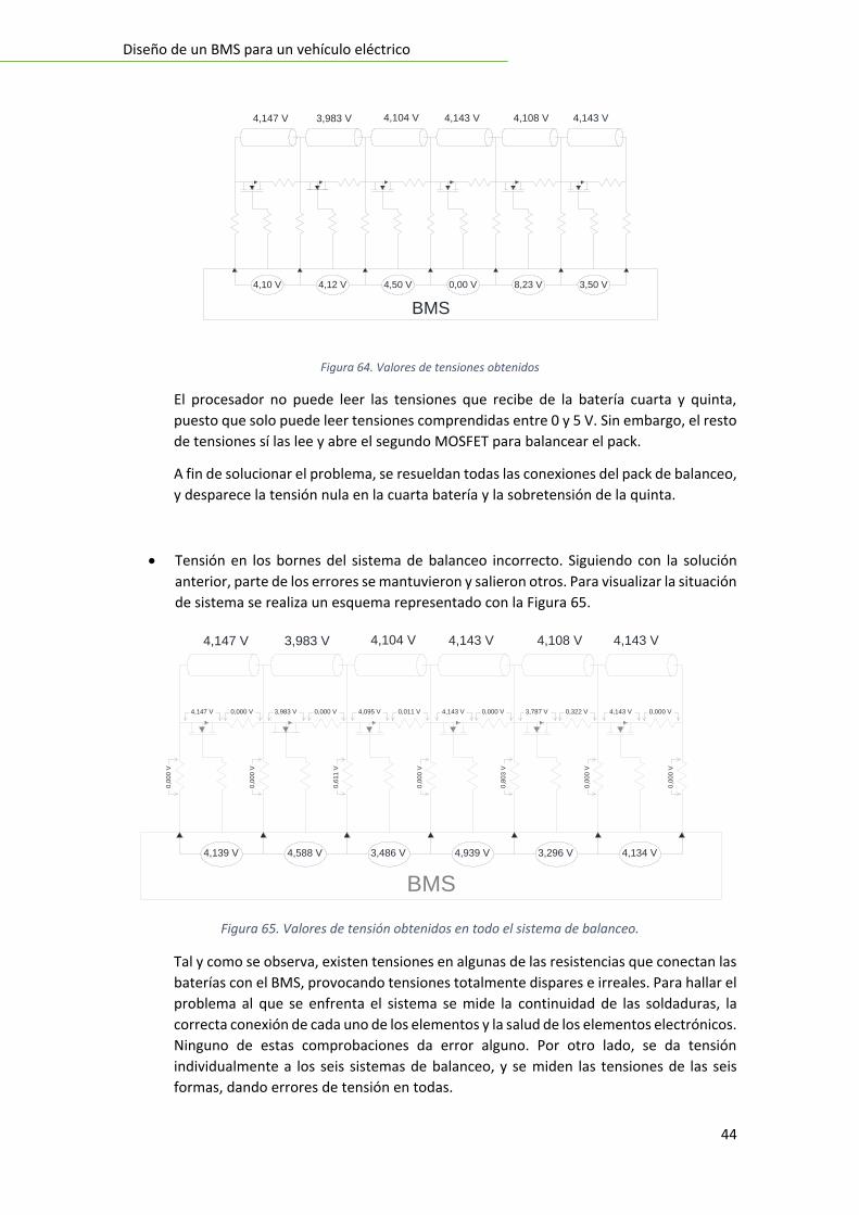
Diseño de un BMS para un vehículo eléctrico
44
Figura 64. Valores de tensiones obtenidos
El procesador no puede leer las tensiones que recibe de la batería cuarta y quinta,
puesto que solo puede leer tensiones comprendidas entre 0 y 5 V. Sin embargo, el resto
de tensiones sí las lee y abre el segundo MOSFET para balancear el pack.
A fin de solucionar el problema, se resueldan todas las conexiones del pack de balanceo,
y desparece la tensión nula en la cuarta batería y la sobretensión de la quinta.
• Tensión en los bornes del sistema de balanceo incorrecto. Siguiendo con la solución
anterior, parte de los errores se mantuvieron y salieron otros. Para visualizar la situación
de sistema se realiza un esquema representado con la Figura 65.
Figura 65. Valores de tensión obtenidos en todo el sistema de balanceo.
Tal y como se observa, existen tensiones en algunas de las resistencias que conectan las
baterías con el BMS, provocando tensiones totalmente dispares e irreales. Para hallar el
problema al que se enfrenta el sistema se mide la continuidad de las soldaduras, la
correcta conexión de cada uno de los elementos y la salud de los elementos electrónicos.
Ninguno de estas comprobaciones da error alguno. Por otro lado, se da tensión
individualmente a los seis sistemas de balanceo, y se miden las tensiones de las seis
formas, dando errores de tensión en todas.
4,147 V
BMS
4,10 V 4,12 V 4,50 V 0,00 V 8,23 V 3,50 V
3,983 V 4,104 V 4,143 V 4,108 V 4,143 V
4,147 V
BMS
3,983 V 4,104 V 4,143 V 4,108 V 4,143 V
4,139 V 4,588 V 3,486 V 4,939 V 3,296 V 4,134 V
4,147 V 0,000 V 3,983 V 0,000 V 4,095 V 0,011 V 4,143 V 0,000 V 3,787 V 0,322 V 4,143 V 0,000 V
0,0
00
V
0,6
11
V
0,0
00
V
0,8
03
V
0,0
00
V
0,0
00
V
0,0
00
V

Diseño de un BMS para un vehículo eléctrico
45
Se desuelda el sistema de balanceo del microchip-master, se da tensión al sistema de
balanceo y se vuelen a medir todas las tensiones. Siguen existiendo incoherencias en las
tensiones que conectarían al microchip y en las resistencias, aunque levemente
modificadas, así que el error no proviene de este último. Se comprueba el correcto
diseño del sistema de balanceo mediante el software LTspice XVII, que muestra un
sistema que debería estar equilibrado y sin errores. Así pues, suponiendo un error de
soldadura, se desuelda todo el sistema de balanceo pasivo y se reconstruye. Los valores
de tensión que se obtienen tras esto siguen siendo erróneos, aunque se acercan a unos
valores más correctos.
Del mismo modo ocurre con el resto de sistemas de balanceo del resto de microchips.
No obstante, los microchips siguen intentando abrir los sistemas de balanceo de las
baterías con mayor tensión que se encuentren en el rango de lectura, pese a que ello no
resulte en abrir el MOSFET deseado o en abrirlo tan siquiera.
• Para que un sistema de balanceo pueda ser llamado BMS debe poder comunicar la
información de las tensiones, temperaturas o cualquier otra información que obtenga,
a otro sistema mediante un puerto o bus de comunicación. El microchip AD7280A
contiene un sistema de comunicación con el que se puede comunicar mediante el
protocolo SPI (Serial Peripheral Interface), unos de los protocolos de 8-bits más sencillos
y usados. Para ayudar al desarrollo existe una base del código para conectar el sistema
a un ordenador en base Linux.
Debido a la dificultad que esto presenta para alguien sin conocimientos sobre el campo,
se pidió ayuda a la propia Analog Devices, responsable del microchip, y a su “Foro de
ingeniería”. Sin embargo, esta fue su respuesta:
“Hello
From your info, and the project that you are taken on, is a bit of a challenge for an
undergraduate. Bottom line is your SPI requires isolation and BMS algorithm. My best
advice is to use our eval-board, check the schematics, the layout, the design, and see
how is done, from this you can learn and re-engineer what’s required. Often the BM
coding are propriety and is specific to each applications/customer, designers tends to
write their own BMS.
If not already done so, May I suggest you have a look at the below eval-board, the IC
parts, demo video/boards, user guides in order to familiarize the applications and to get
some insights. But more specifically to realize the complexity of this project. it is
advisable you reach out to your university supervisor for adequate direction if you're
planning in going down this route.
Regards,
Ching”

Diseño de un BMS para un vehículo eléctrico
46
Traducción:
"Hola
Según su información y el proyecto en el que se encuentra, es un desafío para un
estudiante sin el grado universitario. Para un resultado óptimo, el SPI requiere
aislamiento del BMS y un algoritmo adecuado. Mi mejor consejo es utilizar nuestra placa
de evaluación, verificar los esquemas, el diseño y ver cómo se hace, de esto puede
aprender y rediseñar lo que se requiere. A menudo, la codificación BMS es de propiedad
y es específica para cada aplicación / cliente, los diseñadores tienden a escribir su propio
BMS.
Si aún no lo ha hecho, le sugiero que eche un vistazo a la siguiente tabla de evaluación,
las partes de IC, video / placas de demostración, guías de usuario para familiarizarse con
las aplicaciones y obtener algunas ideas. Pero más específicamente para darse cuenta
de la complejidad de este proyecto. Es aconsejable que se comunique con el tutor de su
proyecto para obtener la dirección adecuada si planea seguir esta ruta.
Saludos,
Ching "
Se intentó realizar el código en Arduino gracias a una plantilla hecha para un AD7280A
junto con su librería específica. Una vez se completó el código el sistema no compilaba
por un error en la librería, un código muy específico que presenta gran dificultad para
alguien sin conocimientos en el área.
Resultados
Los resultados obtenidos no son los esperados, pues pese a todos los esfuerzos y horas
dedicadas no se ha conseguido que el sistema funcione correctamente. Los errores obtenidos
debido a los fallos de soldadura, junto con el extenso y enrevesado cableado, han provocado
que el sistema falle con un motivo todavía por descubrir.
Aparentemente el sistema de balanceo está mal diseñado, pese a que el software LTspice XVII
lo respalda completamente. Se cierran circuitos por donde no deberían, aumentando y
reduciendo las tensiones que mide el microchip de las baterías, por lo que en algunos casos éste
lee que hay baterías con 4.9V (cuando eso es técnicamente imposible sin riesgo) y otras con 3.2
V (Figura 62).
El microchip obtiene todos los parámetros de tensión en los rangos de valores que aparecen en
el datasheet, tal y como aparecen en las siguientes tablas:

Diseño de un BMS para un vehículo eléctrico
47
Parámetro del máster Valor obtenido8 (V) Valor según fabricante (V)
VDD 23.21 8 – 30
VREF 2.508 2.494 - 2.506
VREG 5.206 5.2
CBx 4.957 5
AGND 0 0 – 0.3
AUXx 5.102 5
DGND 0 0 – 0.3
AVCC 5.251 4.9 – 5.5 Tabla 9. Valores de los parámetros del máster.
Parámetro del slave 1 Valor obtenido (V) Valor según fabricante (V)
VDD 24.78 8 – 30
VREF 2.510 2.494 - 2.506
VREG 5.196 5.2
CBx 4.956 5
AGND 0.001 0 – 0.3
AUXx 4.997 5
DGND 0.001 0 – 0.3
AVCC 5.030 4.9 – 5.5 Tabla 10. Valores de los parámetros del slave 1.
Parámetro del slave 2 Valor obtenido (V) Valor según fabricante (V)
VDD 14.47 8 – 30
VREF 2.499 2.494 - 2.506
VREG 5.201 5.2
CBx 5.001 5
AGND 0.002 0 – 0.3
AUXx 5.057 5
DGND 0.002 0 – 0.3
AVCC 5.254 4.9 – 5.5 Tabla 11. Valores de los parámetros del slave 2.
Como únicamente fallan las lecturas que obtiene el microchip, este es capaz de enviar los 5V
necesarios para que se cierre la puerta del MOSFET donde lee más tensión. No obstante, debido
al caos en el que se encuentra el sistema de balanceo, en la mayoría de casos esa tensión no es
suficiente para abrir el MOSFET o es derivada a otras zonas del sistema. Por este motivo se ha
pensado en simplificar el circuito de balanceo eliminando condensadores y todas las resistencias
excepto la de quemado. Sin embargo, la eliminación de las resistencias podría provocar una
enorme subida de intensidad entrante al microchip, pudiendo llegar a destruirlo.
Mejora del sistema
Debido a los diferentes errores que el sistema presenta, se especulan algunas de las mejoras
que podría tener tanto su diseño como su fabricación. La primera de estas mejorar es la
sustitución de las placas PCB de agujero pasante estándar por una placa PCB hecha a medida
con las líneas de conexión ya hechas a falta de la soldadura de los componentes. Esta placa
8 Los valores medidos tienen un error de medida provocado por el multímetro, tiendo éste una resolución de 0.001V y un error de ±(1% + 3 vueltas).

Diseño de un BMS para un vehículo eléctrico
48
aumentaría considerablemente las posibilidades del sistema, eliminando casi todos los errores
que se han encontrado. Sin embargo, el precio de un elemento así ronda los 250 €.
Por otro lado, la compra de un horno de soldadura ayudaría al correcto montaje de todo el
sistema. Este elemento tiene un coste aproximado de entre 250 € y 400 €, sin embargo, algunos
fabricantes de placas PCB ofrecen la posibilidad de montarte ellos mismos los componentes en
las placas, aumentando el coste del pedido, para nuestra situación, de 180 €. Dependiendo del
número de placas sale más rentable la compra de un horno o el montaje por parte del fabricante.
Para completar el sistema, y que técnicamente pueda ser un Battery Management System, se
debe realizar el software que acompaña al microchip AD7280A. Este software en un código que
permite la exportación e importación de datos del microchip a un ordenador u otro sistema,
mediante el protocolo SPI (Serial Peripheral Interface). Una vez este paso esté realizado
correctamente, al sistema se le puede añadir termistores para proteger al pack de la
temperatura, medidores de intensidad, y casi cualquier sistema que complemente y ayude a la
salud del pack mediante datos.
Presupuesto
El coste de los materiales necesarios para construir el sistema presentado es el siguiente:
Componente Unidades Precio (€) Total Vendedor
AD7280ABSTZ 3.00 8.71 26.13 Mouser Electronics
Adaptador QFN48 10.00 0.15 1.48 Aliexpress
Arduino CH340G 1.00 2.31 2.31 Aliexpress
Breadboad PCB 9x15 cm 2.00 0.26 0.52 Aliexpress
Cabezales conexión estándar 2.00 0.98 1.96 Aliexpress
Cableado 1.00 4.07 4.07 Aliexpress
Condensador 0.1µF 32.00 0.09 2.79 Mouser Electronics
Condensador 1µF 6.00 0.25 1.47 Mouser Electronics
Condensador 10µF 3.00 0.20 0.61 Mouser Electronics
Condensador 22pF 18.00 0.09 1.57 Mouser Electronics
LED 20.00 0.04 0.70 Aliexpress
MOSFET 2N7000-G 18.00 0.33 5.91 Mouser Electronics
Punta soldadura 900M-IS 1.00 1.76 1.76 Aliexpress
Resistencia 10kΩ 50.00 0.03 1.65 Mouser Electronics
Resistencia 1kΩ 5.00 0.01 0.05 Aliexpress
Resistencia 20Ω 3.00 0.01 0.03 Aliexpress
Resistencia 30Ω 20.00 0.14 2.70 Mouser Electronics
Rollo estaño 50g 0.5mm 1.00 2.82 2.82 Aliexpress
Soldador 1.00 5.40 5.40 Aliexpress
Terminales 20.00 0.05 0.91 Aliexpress
Tornillos 3x30mm 1.00 2.67 2.67 Leroy Merlin
TOTAL (€) 67.51
IVA (21%) (€) 14.17
TOTAL CON IVA (€) 81.68
Tabla 12. Coste de los componentes para la construcción del BMS.

Diseño de un BMS para un vehículo eléctrico
49
El total de materiales del BMS corresponde a 67.51 €. Sin embargo, si se quisiera realizar una
producción mínima del producto, se aconseja cambiar el presupuesto, y añadir el coste de una
placa PCB a medida (aproximadamente unos 200€) junto con un horno de soldadura
(aproximadamente 350 €), aunque este último al tratarse de maquinaria, su precio se dividiría
según la amortización.
Por otro lado, el coste de construcción de un pack de baterías mínimo y totalmente configurable,
tal y como se ha hecho en este proyecto, tiene un coste de 59.52 €.
Componente Precio (€) Unidades Total Vendedor
Batería litio Samsung ICR18650-26J
3.38 16 54.08 Nkon.nl
Adaptador formato 18650 0.34 16 5.44 Aliexpress
TOTAL (€) 59.52
IVA (21%) (€) 12.49
TOTAL CON IVA (€) 72.02
Tabla 13. Coste de los componentes para la construcción del pack de baterías.
Respecto al coste de ingeniería y desarrollo, suponiendo un solo ingeniero a 30€/h, alcanzaría
un coste de 4800 € brutos. Sin embargo, el sistema no estaría completo sin la inclusión de un
ingeniero informático o un ingeniero de telecomunicaciones para desarrollar las
comunicaciones entre el BMS y el microprocesador (Arduino u otros), aumentando el coste
considerablemente.
Tarea Tiempo invertido (h) Precio (€)
Aprendizaje 30 900
Diseño 60 1800
Construcción 45 1350
Solución de errores 25 750
TOTAL (€) 160 4800 Tabla 14. División del tiempo de trabajo.
Finalmente, el precio total del sistema presentado sería de 4.928,03 €.
Elementos Precio (€)
Materiales BMS 67,51
Pack de baterías 59,52
Ingeniero 4.800,00
TOTAL (€) 4.928,03 Tabla 15. Coste total del proyecto.
Comparación con otros productos
Por mi experiencia personal en mundo laboral, cuando una empresa necesita un BMS construido
por una empresa externa, busca un elemento que sea totalmente configurable, fácil de instalar,
pero sobre todo busca un precio asequible. En el mercado existen diferentes propuestas

Diseño de un BMS para un vehículo eléctrico
50
totalmente opuestas. Por un lado, tenemos los BMS de diseño y construcción china, cuyo precio
no sobrepasa los 50€ pero tiene la desventaja de no ser nada configurables ni adaptables debido
a su morfología centralizada, y por tanto potencia limitada. Al otro lado se encuentran los BMS
diseñados y fabricados en Estados Unidos, Europa y algunas empresas chinas. Dichos productos
son muy atractivos y ofrecen innumerables opciones de personalización y configuración, aunque
el precio suele estar entre las 5 y las 10 veces del coste de un centralizado chino.
Uno de los objetivos principales del presente proyecto era la construcción de un BMS adaptable
cuyo precio no fuese prohibitivo, y que permitiese a cualquier usuario poder manejar este tipo
de tecnología.
Suponiendo el correcto funcionamiento de nuestro BMS, junto con el sistema de comunicación
SPI que le permitiría comunicarse con otros sistemas, lo comparamos con los BMS más
funcionales, económicos y populares del mercado para 16 celdas en serie.
Compañía Modelo Topología Precio (€)
Presente TFG - Modular 67.51
Presente TFG Incluyendo mejoras propuestas9 Modular 370.25
123 Electric 123 Electric Distribuido 894.60
Clean Power Mini BMS Centralizado 221.40
Elecyr Cellcard Master-Slave 382.50
Manzanita Micro MK3x4SMT Master-Slave 765.00
Elithion Lithiumate Lite Distribuido 504.00
Elithion Lithiumate Pro Distribuido 931.50
ACTIA I+ME xNet α Master-Slave 777.60
Zeva EVMS3 Master-Slave 414.80
Tabla 16. Listado de otros sistemas BMS en comparación con el nuestro.
Todos los precios no incluyen IVA.
Como se observa en la tabla comparativa, algunos de los precios de los BMS superan los 500€
fácilmente para solo 16 baterías en serie.
Para una empresa desarrollar un BMS para un solo proyecto no es rentable, pues a los precios
mostrados habría que sumarles el precio del ingeniero y un ingeniero
informático/telecomunicaciones, pero para grandes proyectos la rentabilidad respecto a los
sistemas externos aumenta considerablemente.
9 En este modelo supuesto se ha incluido el precio de una placa PCB a medida, montaje, termistores, un microprocesador integrado (similar al Arduino) y un toroidal para la medida de la corriente.

Diseño de un BMS para un vehículo eléctrico
51
Construcción de un cargador integrado en el BMS
A fin de realizar un sistema completo que fuese capaz tanto de proteger como de cargas las
baterías automáticamente, se propuso la inclusión en el sistema BMS de un cargador para el
pack de baterías.
El cargador, formado por pequeños cargadores encargados de cargar cada uno dos baterías en
serie, estaría soldado en la zona inferior de la segunda placa PCB. Los pequeños cargadores
estarían formados por microchips MCP73213-B6SI/MF, de la compañía Microchip, los cuales son
capaces de cargar automáticamente dos baterías en serie con hasta 1,1 Amperio de intensidad.
Sorprende tanta potencia en un empaquetamiento DIF10, el cual tiene forma cuadrada, 3mm
de lado (Figura 66), y 8 pines de soldadura inferiores (es decir, que no son visibles desde la parte
superior) (Figura 67).
Figura 66. Modelo MCP7 frente a una regla de
medir en cm. Se comprueba que sus lados miden
3mm.
Figura 67. A la izquierda el microchip ya
soldado; a la derecha el propio adaptador.
Respecto al diseño de la electrónica que rodea al chip se puede decir que es básica, sencilla y
fácil de calcular (Figura 68). Según el valor de una de las resistencias se puede comunicar al chip
con que intensidad queremos que trabaje, pudiendo trabajar desde los 100mA hasta 1.1 A.
Figura 68. Esquema eléctrico de un microchip de carga.
El número de chip que se encontrarían en la placa PCB sería de 8, pues se encuentran 16 baterías
en serie, y como se ha dicho, cada chip carga dos de estas baterías.
Esta serie de microchips de carga en concreto tienen una serie de ventajas que otros nos poseen.
La primera de ellas es la comunicación de su funcionamiento mediante un LED. Si funcionaba
todo perfecto, el LED encendía, si se terminaba la carga el LED se mantenía apagado; pero si la
batería o el sistema detecta un error, el LED parpadeaba constantemente. Esto permite al
usuario identificar los errores fácilmente.

Diseño de un BMS para un vehículo eléctrico
52
El sistema de carga se llegó a diseñar y se comprobó el funcionamiento de cada chip por
separado (Figura 69). Los resultados de carga de los chips fueron muy positivos, y la única
dificultad que presentan fue la soldadura a los adaptadores.
Figura 69. Comprobación del funcionamiento del chip. A la izquierda las baterías cargándose, y a la derecha una batería junto a un boost haciendo de fuente de alimentación para el chip.
Estos chips se alimentan mediante una fuente externa, cuyos valores de tensión pueden ser
desde los 8 hasta los 14V. El sistema de alimentación para el sistema de carga formado por estos
microchips seria mediante una fuente de alimentación de ordenador, cuyo carril de 12V es capaz
de producir más de 50 A, por lo que sería más que suficiente para los 8 amperios de carga total
que se necesitan. La Figura 70 representa el diseño propuesto.
Sin embargo, una vez se comenzaron a soldar los elementos a la placa PCB se descubrió que el
sistema estaba completamente mal diseñado, y su funcionamiento comprometido.
Figura 70. Comprobación de funcionamiento de un chip soldado a la placa PCB.
Este hecho se debe a que los microchips necesitan un diferencial de tensión de +12V para poder
funcionar y cargar las baterías, por lo que en una conexión directa, el segundo cargador solo
recibe un máximo de +5V (12V en el positivo y 7V en la parte negativa), y el tercer cargador
recibiría una tensión máxima de -2V ((12V en el positivo y 14V en la parte negativa). En cambio,
si se incluye un optoacoplador u otro elemento que aísle circuitos, los microchips siempre
recibirán +12V en su entrada de tensión (Figura 71).

Diseño de un BMS para un vehículo eléctrico
53
Figura 71. Sistema (a) sin separación de circuitos. Sistema (b) con circuitos separados.
Finalmente se eliminó este apartado del presente Proyecto Final de Carrera.
12 V
DC
Vin
GND
Vout
GND
Vin
GND
Vout
GND
Aislador MCP73213-B6
Vin
GND
Vout
GND
Vin
GND
Vout
GND
Aislador MCP73213-B6
Vin
GND
Vout
GND
Vin
GND
Vout
GND
Aislador MCP73213-B6
12 V
DC
Vin
GND
Vout
GND
MCP73213-B6
Vin
GND
Vout
GND
MCP73213-B6
Vin
GND
Vout
GND
MCP73213-B6
(a) (b)

PLANOS
Plano placa PCB máster
Plano placa PCB sistema de balanceo slaves

AD7280A AD7280A
CS
PD
SDO
SCLK
SDI
CNVST
ALERT
R
1k
R
10k
R
10k
R
10k
2N7000G
R
10k
0.1uF
2N7000G
R
10k
0.1uF
2N7000G
R
10k
0.1uF
R
10k
2N7000G
R
10k
0.1uF
2N7000G
R
10k
0.1uF
2N7000G
R
10k
0.1uF
10uF
0.1uF
0.1uF
AD7280A
1
2
3579
11
12
13
14
1516
17
18
19
20
2122
23 24
25
26
27 29
2830 32 34 36
353331
3738
3940
42 41
44 43
46 45
48 47
1
2
3579
11
12
13
14
1516
17
18
19
20
2122
23 24
25
26
27 29
2830 32 34 36
353331
3738
3940
42 41
44 43
46 45
48 47
1
2
3579
11
12
13
14
1516
17
18
19
20
2122
23 24
25
26
27 29
2830 32 34 36
353331
3738
3940
42 41
44 43
46 45
48 47
10uF
0.1uF
0.1uF
R
1k
R
1k
R
10k
R
10k
R
10k
R
1k
R
1k
R
10k
R
10k
R
10k
10uF
0.1uF
0.1uF
R
1k
21
DISEÑO Y CONTRUCCIÓN DE UN BATTERYMANAGEMENT SYSTEM
Valencia, septiembre 2019
Autor: Alberto Castillo RibellesTutor: Francisco Rodríguez Benito Plano
4/1
ESQUEMA ELÉCTRICO PLACA MÁSTEREscala
1

2N7000G
R
10k
0.1uF
2N7000G
R
10k
0.1uF
2N7000G
R
10k
0.1uF
R
10k
2N7000G
R
10k
0.1uF
2N7000G
R
10k
0.1uF
2N7000G
R
10k
0.1uF
2N7000G
R
10k
0.1uF
2N7000G
R
10k
0.1uF
2N7000G
R
10k
0.1uF
R
10k
2N7000G
R
10k
0.1uF
1
2
DISEÑO Y CONTRUCCIÓN DE UN BATTERYMANAGEMENT SYSTEM
Valencia, septiembre 2019
Autor: Alberto Castillo RibellesTutor: Francisco Rodríguez Benito Plano
4/1
ESQUEMA ELÉCTRICO PLACA SLAVESEscala
2
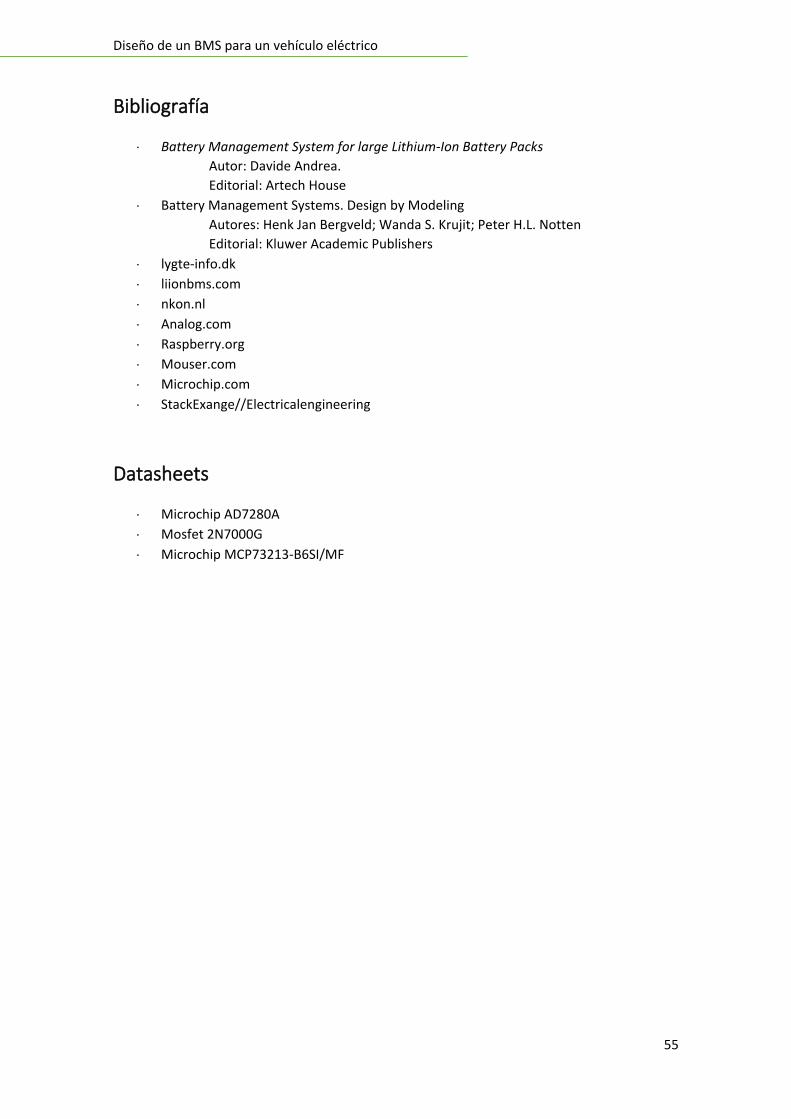
Diseño de un BMS para un vehículo eléctrico
55
Bibliografía
Battery Management System for large Lithium-Ion Battery Packs
Autor: Davide Andrea.
Editorial: Artech House
Battery Management Systems. Design by Modeling
Autores: Henk Jan Bergveld; Wanda S. Krujit; Peter H.L. Notten
Editorial: Kluwer Academic Publishers
lygte-info.dk
liionbms.com
nkon.nl
Analog.com
Raspberry.org
Mouser.com
Microchip.com
StackExange//Electricalengineering
Datasheets
Microchip AD7280A
Mosfet 2N7000G
Microchip MCP73213-B6SI/MF

Lithium Ion Battery Monitoring System AD7280A
Rev. 0 Information furnished by Analog Devices is believed to be accurate and reliable. However, no responsibility is assumed by Analog Devices for its use, nor for any infringements of patents or other rights of third parties that may result from its use. Specifications subject to change without notice. No license is granted by implication or otherwise under any patent or patent rights of Analog Devices. Trademarks and registered trademarks are the property of their respective owners.
One Technology Way, P.O. Box 9106, Norwood, MA 02062-9106, U.S.A.Tel: 781.329.4700 www.analog.com Fax: 781.461.3113 ©2011 Analog Devices, Inc. All rights reserved.
FEATURES 12-bit ADC, 1 μs per channel conversion time 6 analog input channels, common-mode
range 0.5 V to 27.5 V 6 auxiliary ADC inputs ±1.6 mV cell voltage accuracy On-chip voltage regulator Cell balancing interface Daisy-chain interface Internal reference: ±3 ppm/oC 1.8 μA power-down current High input impedance Serial interface with alert function 1 SPI interface for up to 48 channels CRC protection on read and write commands On-chip registers for channel sequencing VDD operating range: 8 V to 30 V Temperature range: −40°C to +105°C 48-lead LQFP Qualified for automotive applications
APPLICATIONS Lithium ion battery monitoring Electric and hybrid electric vehicles Power supply backup Power tools
FUNCTIONAL BLOCK DIAGRAM
CLOCK
2.5VREF
REGULATOR
CELLBALANCINGINTERFACE
DAISY-CHAININTERFACE
AD7280A
12-BIT ADC
VDD
VREG
DGND
DVCC
VSS AGND SDOlo ALERTlo
AVCC
VDRIVE
SCLKSDISDOALERTCSPDCNVSTMASTER
REFGND
CREF
VREF
AUXTERM
LVMUX
AUX6AUX5AUX4AUX3AUX2AUX1
HVMUX
VIN6VIN5VIN4VIN3VIN2VIN1VIN0
SCLK
hiSD
Ihi
SDO
hiA
LER
Thi
CSh
iPD
hiC
NVS
Thi
CB
1C
B2
CB
3C
B4
CB
5C
B6
LIMIT REGSQN LOGIC
DATA MEMORYSPI INTERFACE
CONTROL LOGICAND SELF-TEST
09
43
5-0
01
Figure 1.
GENERAL DESCRIPTION The AD7280A1 contains all the functions required for general-purpose monitoring of stacked lithium ion batteries as used in hybrid electric vehicles, battery backup applications, and power tools. The part has multiplexed cell voltage and auxiliary ADC measurement channels for up to six cells of battery management. An internal ±3 ppm/°C reference is provided that allows a cell voltage accuracy of ±1.6 mV. The ADC resolution is 12 bits and allows conversion of up to 48 cells within 7 μs.
The AD7280A operates from a single VDD supply that has a range of 8 V to 30 V (with an absolute maximum rating of 33 V). The part provides six differential analog input channels to accommodate large common-mode signals across the full VDD range. Each channel allows an input signal range, VIN(+) − VIN(−), of 1 V to 5 V. The input pins assume a series stack of six cells. In addition, the part includes six auxiliary ADC input channels that can be used for temperature measurement or system diagnostics.
The AD7280A includes on-chip registers that allow a sequence of channel measurements to be programmed to suit the application requirements.
The AD7280A also includes a dynamic alert function that can detect whether the cell voltages or auxiliary ADC inputs exceed an upper or lower limit defined by the user. The AD7280A has cell balancing interface outputs designed to control external FET transistors to allow discharging of individual cells.
The AD7280A includes a built-in self-test feature that internally applies a known voltage to the ADC inputs.
A daisy-chain interface allows up to eight parts to be stacked without the need for individual device isolation.
The AD7280A requires only one supply pin that accepts 6.9 mA under normal operation while converting at 1 MSPS.
All this functionality is provided in a 48-lead LQFP package operating over a temperature range of −40°C to +105°C.
1 Patents pending.

AD7280A
Rev. 0 | Page 2 of 48
TABLE OF CONTENTS Features .............................................................................................. 1
Applications ....................................................................................... 1
Functional Block Diagram .............................................................. 1
General Description ......................................................................... 1
Revision History ............................................................................... 2
Specifications ..................................................................................... 3
Power Specifications .................................................................... 5
Timing Specifications .................................................................. 6
Absolute Maximum Ratings ............................................................ 7
Thermal Resistance ...................................................................... 7
ESD Caution .................................................................................. 7
Pin Configuration and Function Descriptions ............................. 8
Typical Performance Characteristics ........................................... 11
Terminology .................................................................................... 14
Theory of Operation ...................................................................... 15
Circuit Information .................................................................... 15
Converter Operation .................................................................. 15
Analog Input Structure .............................................................. 16
Transfer Function ....................................................................... 16
Typical Connection Diagrams .................................................. 17
Reference ..................................................................................... 19
Converting Cell Voltages and Auxiliary ADC Inputs ........... 19
Converting Cell Voltages and Auxiliary ADC Inputs in a Chain of AD7280As ............................................................ 21
Conversion Window .................................................................. 22
Self-Test Conversion .................................................................. 22
Connection of Fewer Than Six Voltage Cells ............................. 22
Auxiliary ADC Inputs ................................................................ 23
Power Requirements .................................................................. 23
Power-Down ............................................................................... 24
Power-Up Time ........................................................................... 25
Cell Balancing Outputs .............................................................. 25
Alert Output ................................................................................ 27
Register Map ................................................................................... 28
Cell Voltage Registers ................................................................ 28
Auxiliary ADC Registers ........................................................... 28
Self-Test Register ........................................................................ 28
Control Register ......................................................................... 28
Cell Overvoltage Register .......................................................... 29
Cell Undervoltage Register ....................................................... 30
AUX ADC Overvoltage Register .............................................. 30
AUX ADC Undervoltage Register ........................................... 30
Alert Register .............................................................................. 30
Cell Balance Register ................................................................. 30
CBx Timer Registers .................................................................. 30
PD Timer Register ...................................................................... 31
Read Register .............................................................................. 31
CNVST Control Register ........................................................... 31
Serial Interface ................................................................................ 32
Writing to the AD7280A ........................................................... 32
Reading from the AD7280A ..................................................... 33
Daisy-Chain Interface .................................................................... 34
Addressing the AD7280A While Reading Back Conversion or Register Data .......................................................................... 34
Initializing the AD7280A .......................................................... 34
Write Acknowledge .................................................................... 35
Cyclic Redundancy Check ........................................................ 35
Examples of Interfacing with the AD7280A ............................... 38
Convert and Readback Routine ............................................... 38
Examples ...................................................................................... 38
EMC Guidelines ............................................................................. 44
Schematic and Layout Guidelines ............................................ 44
Operation in a Noisy Environment ......................................... 44
Software Flowchart .................................................................... 45
Outline Dimensions ....................................................................... 46
Ordering Guide .......................................................................... 46
Automotive Products ................................................................. 46
REVISION HISTORY 4/11—Revision 0: Initial Version

AD7280A
Rev. 0 | Page 3 of 48
SPECIFICATIONS VDD = 8 V to 30 V, VSS = 0 V, DVCC = AVCC = VREG, VDRIVE = 2.7 V to 5.5 V, TA = −40°C to +105°C, unless otherwise noted.
Table 1. Parameter Min Typ Max Unit Test Conditions/Comments DC ACCURACY (VIN0 TO VIN6)1
Resolution 12 Bits No missing codes Integral Nonlinearity ±1 LSB Differential Nonlinearity ±0.8 LSB Offset Error ±1 LSB Offset Error Match 1 LSB Gain Error ±1 LSB Gain Error Match 1 LSB ADC Unadjusted Error2, 3
±1.2 mV Total Unadjusted Error4, 5
±9 mV VIN range6 = 1 V to 4.1 V, −10°C to +85°C ±10 mV VIN range6 = 1 V to 4.1 V, −40°C to +85°C ±1.6 ±14.5 mV VIN range6 = 1 V to 4.1 V, −40°C to +105°C CELL VOLTAGE INPUTS (VIN0 TO VIN6)
Pseudo Differential Input Voltage VIN(x) − VIN(x − 1) 1 2 × VREF V
Absolute Input Voltage VCM − VREF VCM + VREF V Common-Mode Input Voltage 0.5 27.5 V Static Leakage Current7
±5 ±70 nA Dynamic Leakage Current7 ±3 nA CNVST pulse every 100 ms
Input Capacitance 15 pF DC ACCURACY (AUX1 TO AUX6)1, 8
Resolution 12 Bits No missing codes Integral Nonlinearity ±1 LSB Differential Nonlinearity ±0.8 LSB Offset Error ±2 LSB Offset Error Match 2 LSB Gain Error ±2 LSB Gain Error Match 2 LSB ADC Unadjusted Error9 ±1.2 mV Total Unadjusted Error10 ±20 mV −40°C to +85°C
±1.6 ±22 mV −40°C to +105°C AUXILIARY ADC INPUTS (AUX1 TO AUX6)
Input Voltage Range 0 2 × VREF V Static Leakage Current7
±15 nA Dynamic Leakage Current7
±3 nA CNVST pulse every 100 ms
Input Capacitance 15 pF REFERENCE
Reference Voltage 2.494 2.5 2.506 V −40°C to +85°C 2.494 2.5 2.509 V −40°C to +105°C Reference Voltage Temperature
Coefficient ±3 ±15 ppm/°C −40°C to +85°C
±11 ppm/°C −40°C to +105°C Output Voltage Hysteresis 50 ppm −40°C to +105°C Long-Term Drift 150 ppm/1000
hours
Line Regulation ±5 ppm/V Turn-On Settling Time11, 12 5.5 10 ms VREG = 1 μF, VREF = 1 μF, CREF = 100 nF

AD7280A
Rev. 0 | Page 4 of 48
Parameter Min Typ Max Unit Test Conditions/Comments REGULATOR OUTPUT (VREG)
Input Voltage Range 8 30 V Output Voltage, VREG
13 4.9 5.2 5.5 V 5 mA external load Output Current14 5 mA Line Regulation 0.5 mV/V Load Regulation 2.5 mV/mA Internal Short Protection Limit 25 mA For a 10 Ω short
CELL BALANCING OUTPUTS15 Output High Voltage, VOH VREG − 1 5 VREG + 0.2 V ISOURCE = 415 nA Output Low Voltage, VOL 0 V CB1 Output Ramp-Up Time16 30 μs For an 80 pF load CB1 Output Ramp-Down Time17 30 μs For an 80 pF load CB2 to CB6 Output Ramp-Up Time16
380 μs For an 80 pF load CB2 to CB6 Output Ramp-Down Time17
30 μs For an 80 pF load LOGIC INPUTS
Input High Voltage, VINH 2.4 V Input Low Voltage, VINL 0.4 V Input Current, IIN ±10 μA Input Capacitance, CIN 5 pF
LOGIC OUTPUTS Output High Voltage, VOH VDRIVE × 0.9 V ISOURCE = 200 μA Output Low Voltage, VOL 0.4 V ISINK = 200 μA Floating State Leakage Current ±10 μA Floating State Output Capacitance 5 pF Output Coding Straight binary
1 For dc accuracy specifications, the LSB size for cell voltage measurements is (2 × VREF − 1 V)/4096. The LSB size for auxiliary ADC input voltage measurements is (2 × VREF)/4096. 2 ADC unadjusted error includes the INL of the ADC and the gain and offset errors of the VIN0 to VIN6 input channels. 3 The conversion accuracy during cell balancing is decreased due to the activation of the cell balance circuitry. The ADC unadjusted error increases by a factor of 4. 4 Total unadjusted error includes the INL of the ADC and the gain and offset errors of the VIN0 to VIN6 input channels, as well as the reference error, that is, the difference between
the ideal and actual reference voltage and the temperature coefficient of the 2.5 V reference. 5 The conversion accuracy during cell balancing is decreased due to the activation of the cell balance circuitry. The total unadjusted error increases by a factor of 4. 6 For the full analog input range, that is, 1 V to 2 × VREF, the total unadjusted error increases by 20%. 7 The total current measured on the input pins while converting is the sum of the static and dynamic leakage currents. See the Terminology section. 8 Bit D3 of the control register is set to 0 (thermistor termination resistor function is not in use). 9 ADC unadjusted error includes the INL of the ADC and the gain and offset errors of the AUXx input channels. 10 Total unadjusted error includes the INL of the ADC and the gain and offset errors of the AUXx input channels, as well as the reference error, that is, the difference between the
ideal and actual reference voltage and the temperature coefficient of the 2.5 V reference. 11 The turn-on settling time is the time from the rising edge of the PD signal until the conversion result settles to the specified accuracy. This includes the time required
to power up the regulator and the reference. Note that a rising edge on the CNVST input is also required to power up the reference. This rising edge should occur after the rising edge on PD.
12 Sample tested during initial release to ensure compliance. 13 The regulator output voltage is specified with an external 5 mA load in addition to the current required to drive the AVCC, DVCC, and VDRIVE supplies of the AD7280A. 14 This specification refers to the maximum regulator output current that is available for external use. 15 The CBx outputs can be set to 0 V or VREG with respect to the negative terminal of the cell being balanced. 16 The CB1 to CB6 output ramp-up times are defined from the rising edge of the CS command until the CB output exceeds VREG − 1 V with respect to the negative
terminal of the cell being balanced. 17 The CB1 to CB6 output ramp-down times are defined from the rising edge of the CS command until the CB output falls below 50 mV with respect to the negative
terminal of the cell being balanced.

AD7280A
Rev. 0 | Page 5 of 48
POWER SPECIFICATIONS VDD = 8 V to 30 V, VSS = 0 V, DVCC = AVCC = VREG, VDRIVE = 2.7 V to 5.5 V, TA = −40°C to +105°C, unless otherwise noted.
Table 2. Parameter Min Typ Max Unit Test Conditions/Comments POWER REQUIREMENTS
VDD 8 30 V Master Device
IDD During Conversion 5.6 7.3 mA IDD During Data Readback 5.3 7.0 mA IDD During Cell Balancing 5.1 6.8 mA IDD Software Power-Down 2.5 2.9 mA IDD Full Power-Down Mode 1.8 5 μA
Slave Device IDD During Conversion 6.9 8.7 mA IDD During Data Readback 6.5 8.2 mA IDD During Cell Balancing 6.4 8.0 mA IDD Software Power-Down 3.8 4.2 mA IDD Full Power-Down Mode 1.8 5 μA
POWER DISSIPATION Master Device VDD = 30 V
During Conversion 170 220 mW During Data Readback 160 210 mW During Cell Balancing 155 205 mW Software Power-Down 75 90 mW Full Power-Down Mode 54 150 μW
Slave Device VDD = 30 V During Conversion 210 265 mW During Data Readback 195 250 mW During Cell Balancing 192 240 mW Software Power-Down 115 130 mW Full Power-Down Mode 54 150 μW

AD7280A
Rev. 0 | Page 6 of 48
TIMING SPECIFICATIONS VDD = 8 V to 30 V, VSS = 0 V, DVCC = AVCC = VREG, VDRIVE = 2.7 V to 5.5 V, TA = −40°C to +105°C, unless otherwise noted.
Table 3. Parameter1 Min Typ Max Unit Description tCONV ADC conversion time 425 560 695 ns −40°C to +85°C 425 720 ns −40°C to +105°C tACQ ADC acquisition time, Bits[D6:D5] of the control register set to 00 340 400 465 ns −40°C to +85°C 340 470 ns −40°C to +105°C tACQ ADC acquisition time, Bits[D6:D5] of the control register set to 01 665 800 1010 ns −40°C to +85°C 665 1030 ns −40°C to +105°C tACQ ADC acquisition time, Bits[D6:D5] of the control register set to 10 1005 1200 1460 ns −40°C to +85°C 1005 1510 ns −40°C to +105°C tACQ ADC acquisition time, Bits[D6:D5] of the control register set to 11 1340 1600 1890 ns −40°C to +85°C 1340 1945 ns −40°C to +105°C tDELAY 200 250 ns Propagation delay between the falling edges of CNVST of adjacent
parts in the daisy chain tWAIT 5 μs Time required between the end of conversions and the beginning
of readback of the conversion results fSCLK 1 MHz Frequency of serial read clock tQUIET 200 ns Minimum quiet time required between the end of a serial read and
the start of the next conversion t1
2 0.4 50 μs CNVST low pulse
t2 10 ns CS falling edge to SCLK rising edge
t3 20 ns Delay from CS falling edge until SDO is three-state disabled
t4 5 ns SDI setup time prior to SCLK falling edge t5 4 ns SDI hold time after SCLK falling edge t6
3 28 ns Data access time after SCLK rising edge t7 20 ns SCLK to data valid hold time t8 0.45 × tSCLK ns SCLK high pulse width t9 0.45 × tSCLK ns SCLK low pulse width t10
4 100 ns CS rising edge to SCLK rising edge
t11 10 ns CS rising edge to SDO high impedance
t12 3 μs CS high time required between each 32-bit write/read command 1 Sample tested during initial release to ensure compliance. All input signals are specified with tR = tF = 5 ns (10% to 90% of VDRIVE) and timed from a voltage level of 1.6 V.
All timing specifications given are with a 25 pF load capacitance. 2 Maximum allowed CNVST low pulse time to ensure that a software power-down state is not entered when the CNVST pin is not gated. 3 Time required for the output to cross 0.4 V or 2.4 V. 4 t10 applies when using a continuous SCLK. Guaranteed by design.
Timing Diagram
09
43
5-0
20
t8 t10
THREE-STATETHREE-STATE
SCLK
SDO
SDI
LSBMSB MSB – 1
MSB MSB – 1
324321
LSB
t12t2
3t 6t t7
t4 t5
t11t9
CS
Figure 2. Serial Interface Timing Diagram
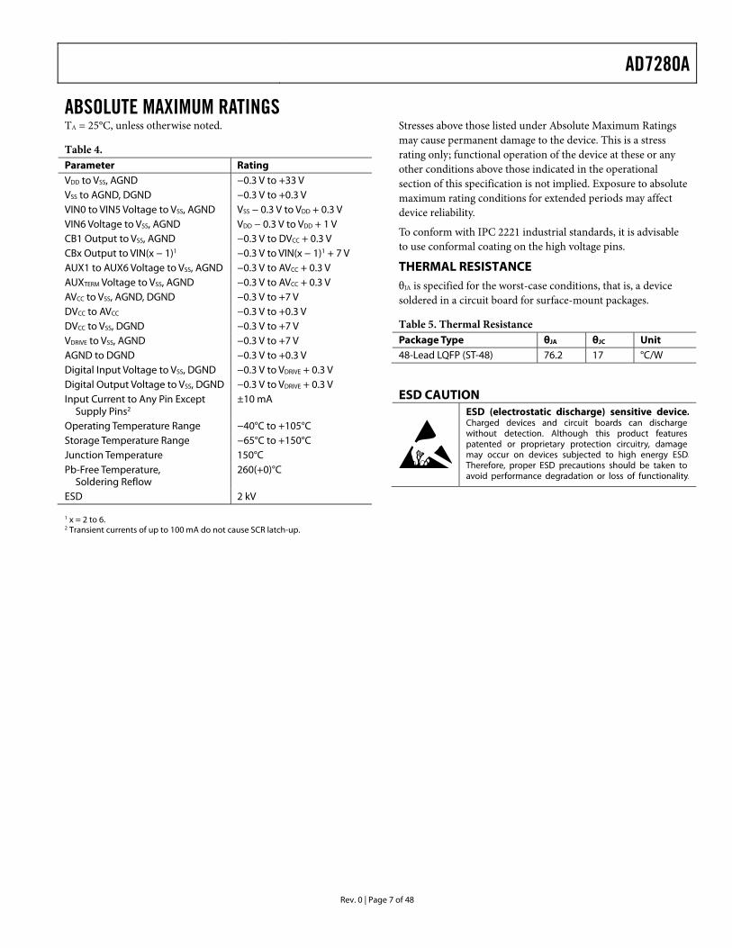
AD7280A
Rev. 0 | Page 7 of 48
ABSOLUTE MAXIMUM RATINGS TA = 25°C, unless otherwise noted.
Table 4. Parameter Rating VDD to VSS, AGND −0.3 V to +33 V VSS to AGND, DGND −0.3 V to +0.3 V VIN0 to VIN5 Voltage to VSS, AGND VSS − 0.3 V to VDD + 0.3 V VIN6 Voltage to VSS, AGND VDD − 0.3 V to VDD + 1 V CB1 Output to VSS, AGND −0.3 V to DVCC + 0.3 V CBx Output to VIN(x − 1)1 −0.3 V to VIN(x − 1)1 + 7 V AUX1 to AUX6 Voltage to VSS, AGND −0.3 V to AVCC + 0.3 V AUXTERM Voltage to VSS, AGND −0.3 V to AVCC + 0.3 V AVCC to VSS, AGND, DGND −0.3 V to +7 V DVCC to AVCC −0.3 V to +0.3 V DVCC to VSS, DGND −0.3 V to +7 V VDRIVE to VSS, AGND −0.3 V to +7 V AGND to DGND −0.3 V to +0.3 V Digital Input Voltage to VSS, DGND −0.3 V to VDRIVE + 0.3 V Digital Output Voltage to VSS, DGND −0.3 V to VDRIVE + 0.3 V Input Current to Any Pin Except
Supply Pins2 ±10 mA
Operating Temperature Range −40°C to +105°C Storage Temperature Range −65°C to +150°C Junction Temperature 150°C Pb-Free Temperature,
Soldering Reflow 260(+0)°C
ESD 2 kV 1 x = 2 to 6. 2 Transient currents of up to 100 mA do not cause SCR latch-up.
Stresses above those listed under Absolute Maximum Ratings may cause permanent damage to the device. This is a stress rating only; functional operation of the device at these or any other conditions above those indicated in the operational section of this specification is not implied. Exposure to absolute maximum rating conditions for extended periods may affect device reliability.
To conform with IPC 2221 industrial standards, it is advisable to use conformal coating on the high voltage pins.
THERMAL RESISTANCE θJA is specified for the worst-case conditions, that is, a device soldered in a circuit board for surface-mount packages.
Table 5. Thermal Resistance Package Type θJA θJC Unit 48-Lead LQFP (ST-48) 76.2 17 °C/W
ESD CAUTION

AD7280A
Rev. 0 | Page 8 of 48
PIN CONFIGURATION AND FUNCTION DESCRIPTIONS
48
PDhi
47
CSh
i
46
SCLK
hi
45
SDO
hi
44
CN
VSTh
i
43
SDIh
i
42
ALE
RTh
i
41
REF
GN
D
40
V REF
39
CR
EF
38
AU
X1
37
AU
X2
35 AUX434 AUX533 AUX6
30 AVCC
31 AGND
32 AUXTERM
36 AUX3
29 VDRIVE28 ALERTlo27 ALERT
25 SDOlo
26 SDO
2CB63VIN54CB5
7VIN3
6CB4
5VIN4
1VIN6
8CB39VIN210CB2
12CB1
11VIN1
13
VIN
0
14
MA
STER
15
PD
16
V DD
17
V SS
18V R
EG19
DV C
C20
DG
ND
21
CS
22
SCLK
23
SDI
24
CN
VST
PIN 1
AD7280ATOP VIEW
(Not to Scale)
094
35-0
03
Figure 3. Pin Configuration
Table 6. Pin Function Descriptions Pin No. Mnemonic Description 1, 3, 5, 7, 9, 11, 13
VIN6 to VIN0 Analog Input 6 to Analog Input 0. VIN0 should be connected to the base of the series-connected battery cells. VIN1 should be connected to the top of Cell 1, VIN2 should be connected to the top of Cell 2, and so on (see Figure 28 and Figure 29).
2, 4, 6, 8, 10, 12
CB6 to CB1 Cell Balance Output 6 to Cell Balance Output 1. These pins provide a voltage output that can be used to supply the gate drive of an external cell balancing transistor. Each CBx output provides a 0 V or 5 V voltage output referenced to the absolute amplitude of the negative terminal of the battery cell that is being balanced.
14 MASTER Voltage Input. Connect the MASTER pin of the AD7280A that is connected directly to the DSP/microprocessor to the VDD supply pin through a 10 kΩ resistor. In an application with two or more AD7280As in a daisy chain, the MASTER pins of the remaining AD7280As in the daisy chain should be tied to their respective VSS supply pins through 10 kΩ resistors.
15 PD Power-Down Input. This input is used to power down the AD7280A. When the AD7280A acts as a master, the PD input is supplied from the DSP/microprocessor. When the AD7280A acts as a slave in a daisy chain, the PD input should be connected to the PDhi output of the AD7280A immediately below it in potential in the daisy chain.
16 VDD Positive Power Supply Voltage for the High Voltage Analog Input Structure of the AD7280A. The supply must be greater than the minimum voltage of 8 V. VDD can be supplied directly from the cell with the highest potential of the four, five, or six cell battery stacks that the AD7280A is monitoring. The maximum voltage that should be applied between VDD and VSS is 30 V. Place 10 μF and 100 nF decoupling capacitors on the VDD pin.
17 VSS Negative Power Supply Voltage for the High Voltage Analog Input Structure of the AD7280A. This input should be at the same potential as the AGND/DGND voltage.
18 VREG Analog Voltage Output, 5.2 V. The internally generated VREG voltage, which provides the supply voltage for the ADC core, is available on this pin for use external to the AD7280A. Place 1 μF and 100 nF decoupling capacitors on the VREG pin.
19 DVCC Digital Supply Voltage, 4.9 V to 5.5 V. The DVCC and AVCC voltages should ideally be at the same potential. For best performance, it is recommended that the DVCC and AVCC pins be shorted together to ensure that the voltage difference between them never exceeds 0.3 V, even on a transient basis. This supply should be decoupled to DGND. Place 100 nF decoupling capacitors on the DVCC pin. The DVCC supply pin should be connected to the VREG output.
20 DGND Digital Ground. Ground reference point for all digital circuitry on the AD7280A. The DGND and AGND voltages should ideally be at the same potential and must not be more than 0.3 V apart, even on a transient basis.

AD7280A
Rev. 0 | Page 9 of 48
Pin No. Mnemonic Description 21 CS Chip Select Input. The CS input is used to frame the input and output data on the SPI and daisy-chain
interfaces. On the master AD7280A device, the CS input is supplied from the DSP/microprocessor. When the AD7280A acts as a slave in a daisy chain, this input should be connected to the CShi output of the AD7280A immediately below it in potential in the daisy chain.
22 SCLK Serial Clock Input. On the master AD7280A device, the SCLK input is supplied from the DSP/microprocessor. When the AD7280A acts as a slave in a daisy chain, this input should be connected to the SCLKhi output of the AD7280A immediately below it in potential in the daisy chain.
23 SDI Serial Data Input. Data to be written to the on-chip registers is provided on this input and is clocked into the AD7280A on the falling edge of the SCLK input. On the master AD7280A device, SDI is the data input of the SPI interface. When the AD7280A acts as a slave in a daisy chain, this input accepts data from the SDOhi output of the AD7280A immediately below it in potential in the daisy chain.
24 CNVST Convert Start Input. The conversion is initiated on the falling edge of CNVST. On the master AD7280A, the CNVST pulse is supplied from the DSP/microprocessor; this input can also be tied to DVCC and the conversion initiated through the serial interface. When the AD7280A acts as a slave in a daisy chain, this input should be connected to the CNVSThi output of the AD7280A immediately below it in potential in the daisy chain.
25 SDOlo Serial Data Output in Daisy-Chain Mode. On the master AD7280A device, this output should be connected to VSS either directly or through a pull-down, 1 kΩ resistor. When the AD7280A acts as a slave in a daisy chain, this output should be connected to the SDIhi input of the AD7280A immediately below it in potential in the daisy chain.
26 SDO Serial Data Output. The conversion output data or the register output data is supplied to this pin as a serial data stream. The bits are clocked out on the rising edge of the SCLK input; 32 SCLKs are required to access the data. On the master AD7280A device, the SDO output should be connected to the DSP/microprocessor. The SDO outputs of the remaining AD7280As in the daisy chain should be connected to VSS either directly or through a pull-down, 1 kΩ resistor.
27 ALERT Digital Output. This flag indicates cell or auxiliary ADC input overvoltage or undervoltage. The ALERT output of the master AD7280A should be connected to the DSP/microprocessor. The ALERT outputs of the remaining AD7280As in the daisy chain should be connected to VSS either directly or through a pull-down, 1 kΩ resistor.
28 ALERTlo Alert Output in Daisy-Chain Mode. On the master AD7280A, this output should be connected to VSS either directly or through a pull-down, 1 kΩ resistor. When the AD7280A acts as a slave in a daisy chain, this output should be connected to the ALERThi input of the AD7280A immediately below it in potential in the daisy chain.
29 VDRIVE Logic Power Supply Input. The voltage supplied at this pin determines the voltage at which the SPI interface operates. This pin should be decoupled to DGND. On the master AD7280A device, the voltage range on this pin is 2.7 V to 5.5 V. The VDRIVE voltage can be different from the voltage at AVCC and DVCC, but it should never exceed either by more than 0.3 V. The VDRIVE pin of the remaining AD7280As in the daisy chain should be connected to VREG.
30 AVCC Analog Supply Voltage for the ADC Core, 4.9 V to 5.5 V. The AVCC and DVCC voltages should ideally be at the same potential. For best performance, it is recommended that the AVCC and DVCC pins be shorted together to ensure that the voltage difference between them never exceeds 0.3 V, even on a transient basis. This supply should be decoupled to AGND. Place 100 nF decoupling capacitors on the AVCC pin. The AVCC supply pin should be connected to the VREG output.
31 AGND Analog Ground. This pin is the ground reference point for all analog circuitry on the AD7280A. This input should be at the same potential as the base of the series-connected battery cells. The AGND and DGND voltages should ideally be at the same potential and must not be more than 0.3 V apart, even on a transient basis.
32 AUXTERM Thermistor Termination Resistor Input. If this function is not required in the application, it is recommended that this pin be connected to VREG through a 10 kΩ resistor.
33 to 38 AUX6 to AUX1 Auxiliary, Single-Ended 5 V ADC Inputs. If any of these inputs is not required in the application, it is recommended that the pin be connected to VREG through a 10 kΩ resistor.
39 CREF Reference Capacitor. A 100 nF decoupling capacitor to REFGND should be placed on this pin. 40 VREF Reference Output, 2.5 V. The on-chip reference is available on this pin for use external to the AD7280A.
A 1 μF decoupling capacitor to REFGND is recommended on this pin. 41 REFGND Reference Ground. This pin is the ground reference point for the internal band gap reference circuitry on
the AD7280A. The REFGND voltage should be at the same potential as the AGND voltage. 42 ALERThi Alert Input in Daisy-Chain Mode. The alert signal from each AD7280A in the daisy chain is passed through
the ALERTlo output and the ALERThi input of each AD7280A in the chain and is supplied to the DSP/micro-processor through the ALERT output of the master AD7280A. This input should be connected to the ALERTlo output of the AD7280A immediately above it in potential in the daisy chain. The AD7280A at the highest potential in the stack does not require an alert input; in this case, the pin should be connected to VDD through a 1 kΩ resistor.

AD7280A
Rev. 0 | Page 10 of 48
Pin No. Mnemonic Description 43 SDIhi Serial Data Input in Daisy-Chain Mode. The data from each AD7280A in the daisy chain is passed through the
SDOlo output and the SDIhi input of each AD7280A in the chain and is supplied to the DSP/microprocessor through the SDO output of the master AD7280A. This input should be connected to the SDOlo output of the AD7280A immediately above it in potential in the daisy chain. The AD7280A at the highest potential in the stack does not require a serial data input in daisy-chain mode; in this case, the pin should be connected to VDD through a 1 kΩ resistor.
44 CNVSThi Conversion Start Output in Daisy-Chain Mode. The convert start signal from the DSP/microprocessor supplied to the CNVST input of the master AD7280A is passed through each AD7280A by means of the CNVST input and the CNVSThi output. This output should be connected to the CNVST pin of the AD7280A immediately above it in potential in the daisy chain. The AD7280A at the highest potential in the stack does not require a daisy-chain conversion start output; in this case, the pin should be connected to VDD.
45 SDOhi Serial Data Output in Daisy-Chain Mode. The serial data input from the DSP/microprocessor supplied to the SDI input of the master AD7280A is passed through each AD7280A by means of the SDI input and the SDOhi output. This output should be connected to the SDI input of the AD7280A immediately above it in potential in the daisy chain. The AD7280A at the highest potential in the stack does not require a daisy-chain serial data output; in this case, the pin should be connected to VDD.
46 SCLKhi Serial Clock Output in Daisy-Chain Mode. The clock signal from the DSP/microprocessor supplied to the SCLK input of the master AD7280A is passed through each AD7280A by means of the SCLK input and the SCLKhi output. This output should be connected to the SCLK input of the AD7280A immediately above it in potential in the daisy chain. The AD7280A at the highest potential in the stack does not require a daisy-chain serial clock output; in this case, the pin should be connected to VDD.
47 CShi Chip Select Output in Daisy-Chain Mode. The chip select signal from the DSP/microprocessor supplied to the CS input of the master AD7280A is passed through each AD7280A by means of the CS input and the CShi output. This output should be connected to the CS input of the AD7280A immediately above it in potential in the daisy chain. The AD7280A at the highest potential in the stack does not require a daisy-chain chip select output; in this case, the pin should be connected to VDD.
48 PDhi Power-Down Output in Daisy-Chain Mode. The power-down signal from the DSP/microprocessor supplied to the PD input of the master AD7280A is passed through each AD7280A by means of the PD input and the PDhi output. This output should be connected to the PD input of the AD7280A immediately above it in potential in the daisy chain. The AD7280A at the highest potential in the stack does not require a daisy-chain power-down output; in this case, the pin should be connected to VDD.

AD7280A
Rev. 0 | Page 11 of 48
TYPICAL PERFORMANCE CHARACTERISTICS
5.5
4.9
5.0
5.1
5.2
5.3
5.4
–40 –20 0 20 40 60 80 100
V REG
VO
LTA
GE
(V)
TEMPERATURE (°C)
VDD = 8VVDD = 10VVDD = 22.5VVDD = 29.9V
094
35
-10
2
8
1
2
4
3
5
6
7
–40 –20 0 20 40 60 80 100
I DD
(mA
)
TEMPERATURE (°C)
SLAVE CURRENTS
MASTER CURRENTS
094
35
-10
5
MASTER, VDD = 8VMASTER, VDD = 10VMASTER, VDD = 29.9V
SLAVE, VDD = 8VSLAVE, VDD = 10VSLAVE, VDD = 29.9V
Figure 4. VREG vs. Temperature for Different Supply Voltages, VREG Connected to AVCC and DVCC
Figure 7. IDD During Cell Balancing vs. Temperature for Different Supply Voltages
5.5
4.9
5.0
5.1
5.2
5.3
5.4
–40 –20 0 20 40 60 80 100
V REG
VO
LTA
GE
(V)
TEMPERATURE (°C)
VDD = 8VVDD = 10VVDD = 22.5VVDD = 29.9V
094
35
-10
3
8
1
2
4
3
5
6
7
–40 –20 0 20 40 60 80 100
I DD
(mA
)
TEMPERATURE (°C)
SLAVE CURRENTS
MASTER CURRENTS
094
35
-10
6
MASTER, VDD = 8VMASTER, VDD = 10VMASTER, VDD = 29.9V
SLAVE, VDD = 8VSLAVE, VDD = 10VSLAVE, VDD = 29.9V
Figure 5. VREG vs. Temperature for Different Supply Voltages, VREG Connected to AVCC and DVCC, 5 mA External Load
Figure 8. IDD During Software Power-Down vs. Temperature for Different Supply Voltages
8
1
2
4
3
5
6
7
–40 –20 0 20 40 60 80 100
I DD
(mA
)
TEMPERATURE (°C)
SLAVE CURRENTS
MASTER CURRENTS
094
35
-10
4
MASTER, VDD = 8VMASTER, VDD = 10VMASTER, VDD = 29.9V
SLAVE, VDD = 8VSLAVE, VDD = 10VSLAVE, VDD = 29.9V
10,000
8000
6000
4000
2000
026682667266626652664
9149
26632662
3864605
26612660
NU
MB
ER O
F O
CC
UR
REN
CES
CODE
094
35
-10
7
Figure 6. IDD During Conversion vs. Temperature for Different Supply Voltages
Figure 9. Histogram of Codes for 10,000 Samples, Odd Cell Voltage Channels

AD7280A
Rev. 0 | Page 12 of 48
266826672666266526642663266226612660CODE
10,000
8000
6000
4000
2000
0
8870
167
956
7
NU
MB
ER O
F O
CC
UR
REN
CES
094
35
-10
8Figure 10. Histogram of Codes for 10,000 Samples,
Even Cell Voltage Channels
10,000
8000
6000
4000
2000
029522951295029492948
236
2947
9072
2946
692
29452943 29442942
NU
MB
ER O
F O
CC
UR
REN
CES
CODE
094
35
-10
9
Figure 11. Histogram of Codes for 10,000 Samples, Auxiliary Channels
–40 –20 0 20 40 60 80 100
V REF
VO
LTA
GE
(V)
TEMPERATURE (°C)
094
35
-21
2
2.496
2.497
2.498
2.499
2.500
2.501
2.502
2.503
2.504
2.505
2.506
2.507
2.508VDD = 8VVDD = 10VVDD = 16.8VVDD = 22.5VVDD = 29.9V
Figure 12. VREF vs. Temperature for Different Supply Voltages
2.496
2.498
2.500
2.502
2.504
2.506
2.508
–40 –20 0 20 40 60 80 100
V REF
VO
LTA
GE
(V)
TEMPERATURE (°C)
PART 1PART 4PART 7PART 10
PART 2PART 5PART 8PART 11
PART 3PART 6PART 9PART 12
094
35
-11
1
Figure 13. VREF vs. Temperature for Different Parts
–40 –20 0 20 40 60 80 100
TOTA
L U
NA
DJU
STED
ER
RO
R (m
V)
TEMPERATURE (°C)
094
35
-21
4
–4.5
–3.0
–1.5
0
1.5
3.0
4.5
6.0
7.5VDD = 8VVDD = 10VVDD = 16.8VVDD = 22.5VVDD = 29.9V
Figure 14. Total Unadjusted Error for Even Cell Voltage Channels (Absolute Value) vs. Temperature for Different Supply Voltages
–40 –20 0 20 40 60 80 100
TOTA
L U
NA
DJU
STED
ER
RO
R (m
V)
TEMPERATURE (°C)
094
35
-21
5
–4.5
–3.0
–1.5
0
1.5
3.0
4.5
6.0
7.5VDD = 8VVDD = 10VVDD = 16.8VVDD = 22.5VVDD = 29.9V
Figure 15. Total Unadjusted Error for Odd Cell Voltage Channels (Absolute Value) vs. Temperature for Different Supply Voltages

AD7280A
Rev. 0 | Page 13 of 48
–40 –20 0 20 40 60 80 100
TOTA
L U
NA
DJU
STED
ER
RO
R (m
V)
TEMPERATURE (°C)
094
35
-21
6
–4.5
–3.0
–1.5
0
1.5
3.0
4.5
6.0
7.5VDD = 8VVDD = 10VVDD = 16.8VVDD = 22.5VVDD = 29.9V
0
5
4
3
2
1
0 2 4 6 8 1
VOLT
AG
E (V
)
TIME (ms)0
PDVREGVREF
094
35
-11
7
Figure 16. Total Unadjusted Error for Auxiliary Channels (Absolute Value) vs. Temperature for Different Supply Voltages
Figure 19. Power-Up Time, 10 μF Capacitor on the VREF and VREG Pins
0
5
4
3
2
1
0 2 4 6 8 1
VOLT
AG
E (V
)
TIME (ms)0
PDVREGVREF
094
35
-11
5 0
5
4
3
2
1
0 2 4 6 8 1
VOLT
AG
E (V
)
TIME (ms)0
PDVREGVREF
094
35
-11
8
Figure 17. Power-Up Time, 1 μF Capacitor on the VREF and VREG Pins Figure 20. Power-Down Time, 10 μF Capacitor on the VREF and VREG Pins
3.2
5.2
4.8
4.4
4.0
3.6
0 8700600500400300200100
CB
x O
UTP
UT
VOLT
AG
E (V
)
LOAD CURRENT (nA)
0
5
4
3
2
1
0 2 4 6 8 1
VOLT
AG
E (V
)
TIME (ms)0
PDVREGVREF
094
35
-11
6
00
094
35
-11
9
Figure 18. Power-Down Time, 1 μF Capacitor on the VREF and VREG Pins Figure 21. CBx Output Voltage vs. Load Current

AD7280A
Rev. 0 | Page 14 of 48
TERMINOLOGY Differential Nonlinearity (DNL) DNL is the difference between the measured and the ideal 1 LSB change between any two adjacent codes in the ADC.
Integral Nonlinearity (INL) INL is the maximum deviation from a straight line passing through the endpoints of the ADC transfer function. The endpoints of the transfer function are zero scale (a point 1 LSB below the first code transition) and full scale (a point 1 LSB above the last code transition).
Offset Error Offset error applies to straight binary output coding. It is the deviation of the first code transition (000 ... 000) to (000 ... 001) from the ideal, that is, AGND + 1 LSB for AUX1 to AUX6 and 1 V + AGND + 1 LSB for VIN0 to VIN6.
Offset Error Match Offset error match is the difference in zero code error across all six channels.
Gain Error Gain error applies to straight binary output coding. It is the deviation of the last code transition (111 ... 110) to (111 ... 111) from the ideal (that is, 2 × VREF − 1 LSB) after adjusting for the offset error.
Gain Error Match Gain error match is the difference in gain error across all six channels.
ADC Unadjusted Error ADC unadjusted error includes the INL error and the offset and gain errors of the ADC and measurement channel.
Total Unadjusted Error (TUE) TUE is the maximum deviation of the output code from the ideal. Total unadjusted error includes the INL error, the offset and gain errors, and the reference errors. Reference errors include the difference between the actual and ideal reference voltage (that is, 2.5 V) and the reference voltage temperature coefficient.
Reference Voltage Temperature Coefficient The reference voltage temperature coefficient is derived from the maximum and minimum reference output voltage (VREF) measured between TMIN and TMAX. It is expressed in ppm/°C using the following equation:
610)(V5.2
)()(C)(ppm/ ×⎟
⎟⎠
⎞⎜⎜⎝
⎛
−×
−=°
MINMAX
REFREFREF TT
MinVMaxVTCV
where: VREF(Max) is the maximum VREF between TMIN and TMAX. VREF(Min) is the minimum VREF between TMIN and TMAX. TMAX = +85°C or +105°C. TMIN = −40°C.
Output Voltage Hysteresis Output voltage hysteresis, or thermal hysteresis, is defined as the absolute maximum change of reference output voltage after the device is cycled through temperature from either T_HYS+ or T_HYS−, where:
T_HYS+ = +25°C to TMAX to +25°C T_HYS− = +25°C to TMIN to +25°C
Output voltage hysteresis is expressed in ppm using the follow-ing equation:
610C)25(
)(C)25((ppm) ×⎟
⎟⎠
⎞⎜⎜⎝
⎛
°
−°=
REF
REFREFHYS V
T_HYSVVV
where: VREF(25°C) = VREF at 25°C. VREF(T_HYS) is the maximum change of VREF at T_HYS+ or T_HYS−.
Static Leakage Current Static leakage current is the current measured on the cell voltage and/or the auxiliary ADC inputs when the device is static, that is, not converting.
Dynamic Leakage Current Dynamic leakage current is the current measured on the cell voltage and/or the auxiliary ADC inputs when the device is converting, with the static leakage current subtracted. Dynamic leakage current is specified with a convert start pulse frequency of 10 Hz, that is, every 100 ms. The dynamic leakage current for a different conversion rate can be calculated using the following equation:
⎟⎟⎠
⎞⎜⎜⎝
⎛ ×=
)(
)(
ACNVST
BCNVSTDYN(A)DYN(B) f
fII
where: IDYN(A) is the dynamic leakage current at the convert start frequency, fCNVST(A) (see Table 1). IDYN(B) is the dynamic leakage current at the desired convert start frequency, fCNVST(B).

AD7280A
Rev. 0 | Page 15 of 48
THEORY OF OPERATION CIRCUIT INFORMATION The AD7280A is a lithium ion (Li-Ion) battery monitoring chip that can monitor the voltage and temperature of four, five, or six series-connected Li-Ion battery cells. The AD7280A also provides an interface that can be used to control external transistors for cell balancing.
The VDD and VSS supplies required by the AD7280A should be taken from battery cells being monitored by the part. An internal VREG rail is generated to provide power for the ADC and the internal interface circuitry. This VREG voltage is available on an output pin for use external to the AD7280A.
The AD7280A consists of a high voltage input multiplexer, a low voltage input multiplexer, and a SAR ADC. The high voltage multiplexer allows four, five, or six series-connected Li-Ion battery cells to be measured. The low voltage multiplexer provides the user with six single-ended ADC inputs that can be used in combination with external thermistors to measure the tempera-ture of each battery cell. The auxiliary ADC inputs can also be used for external diagnostics in the application. Initiating conver-sions on all 12 channels, that is, the six cell voltage channels and the six auxiliary ADC channels, requires only a single CNVST pulse. Alternatively, the conversion can be initiated through the rising edge of CS. Each conversion result is stored in an individual result register (see ). Table 13
Each individual cell voltage and auxiliary ADC measurement requires a minimum of 1 μs to acquire and complete a conver-sion. Depending on the external components connected to the analog inputs of the AD7280A, additional acquisition time may be required. A higher acquisition time can be selected through the control register. The AD7280A also provides a conversion averaging option that can be selected through the control register. This option allows the user to complete two, four, or eight averages on each cell voltage and auxiliary ADC measurement. The aver-aged conversion results are stored in the result registers. On power-up, the default combined acquisition and conversion time is 1 μs, with the averaging register set to 0, that is, a single conversion per channel.
The results of the cell voltage and auxiliary ADC conversions are read back via the 4-wire serial peripheral interface (SPI). The SPI is also used to write to and read from the internal registers.
The AD7280A features an alert function that can be triggered if the voltage conversion results or the auxiliary ADC conversion results exceed the maximum and minimum voltage thresholds selected by the user. The alert modes and threshold levels are selected by writing to internal registers.
The AD7280A provides six analog output voltages that can be used to control external transistors as part of a cell balancing circuit. Each cell balance output provides a 0 V or 5 V voltage, with respect to the potential on the base of each individual cell, that can be applied to the gate of the external cell balancing transistors.
The AD7280A features a daisy-chain interface. Individual AD7280A devices can monitor the cell voltages and tempera-tures of six cells. A chain of AD7280As can be used to monitor the cell voltages and temperatures of a larger number of cells. The conversion data from each AD7280A in the chain passes to the system controller via a single SPI interface. Control data can similarly be passed via the SPI up the chain to each individual AD7280A.
The AD7280A includes an on-chip 2.5 V reference. The reference voltage is available for use external to the AD7280A.
The AD7280A also has a VDRIVE feature to control the voltage at which the serial interface operates. VDRIVE allows the ADC to easily interface to both 3 V and 5 V processors. For example, in the recommended configuration, the AD7280A is operated with a supply of 5 V; however, the VDRIVE pin can be powered from a 3 V supply, allowing a large dynamic range with low voltage digital processors.
CONVERTER OPERATION The conversion paths of the AD7280A consist of a high voltage input multiplexer or a low voltage input multiplexer and a SAR ADC. The high voltage multiplexer selects the pair of analog inputs, VIN0 to VIN6, that is to be converted. The voltage of each individual cell is measured by converting the difference between adjacent analog inputs, that is, VIN1 − VIN0, VIN2 − VIN1, and so on (see Figure 22 and Figure 23). The low voltage multiplexer selects the auxiliary ADC input, AUX1 to AUX6, that is to be converted. The conversion results for each cell voltage and auxiliary ADC input can be accessed tWAIT after the programmed conversion sequence is completed.
VIN6
VIN5
VIN4
VIN3
VIN2
VIN1
VIN0
ADC VIN+
ADC VIN–
09
43
5-0
04
Figure 22. Mux Configuration During VIN1 to VIN0 Sampling

AD7280A
Rev. 0 | Page 16 of 48
VIN6
VIN5
VIN4
VIN3
VIN2
VIN1
VIN0
ADC VIN+
ADC VIN–
09
43
5-0
05
Figure 23. Mux Configuration During VIN2 to VIN1 Sampling
The ADC is a successive approximation register analog-to-digital converter (SAR ADC). The converter is composed of a comparator, a SAR, control logic, and two capacitive DACs. Figure 24 shows a simplified schematic of the converter. During the acquisition phase, the SW1, SW2, and SW3 switches are closed. The sampling capacitor array acquires the signal on the input during this phase.
CAPACITIVEDAC
CAPACITIVEDAC
CONTROLLOGIC
COMPARATOR
SW3SW1SW2
VREF
VREF
VIN+
VIN–
CS
CS
B
A
A
B
09
43
5-0
06
Figure 24. ADC Configuration During Acquisition Phase
When the ADC starts a conversion, SW3 opens, and SW1 and SW2 move to Position B, causing the comparator to become unbalanced (see Figure 25). The control logic and capacitive DACs are used to add and subtract fixed amounts of charge to return the comparator to a balanced condition. When the comparator is rebalanced, the conversion is complete. The control logic gen-erates the ADC output code. This output code is then stored in the appropriate register for the input that has been converted.
CAPACITIVEDAC
CAPACITIVEDAC
CONTROLLOGIC
COMPARATOR
SW3SW1SW2
VREF
VIN+
VIN–
CS
CS
B
A
A
B
VREF
09
43
5-0
07
Figure 25. ADC Configuration During Conversion Phase
ANALOG INPUT STRUCTURE Figure 26 shows the equivalent circuit of the analog input structure of the AD7280A. The diodes provide ESD protection. The resistors are lumped components made up of the on resistance of the input multiplexer, internal track resistance, and other internal switches. The value of these resistors is approximately 300 Ω typical. Capacitor C1 is also a lumped component made up of pin capacitance, ESD diodes, and switch capacitance, whereas Capacitor C2 is the sampling capacitor of the ADC. The total lumped capacitance of C1 and C2 is approximately 15 pF.
C1
C2D
D
R1
VDD
VIN+
VSS
C1
C2D
D
R1
VDD
VIN–
VSS
094
35
-008
Figure 26. Equivalent Analog Input Circuit
TRANSFER FUNCTION The output coding of the AD7280A is straight binary. The designed code transitions occur at successive integer LSB values (that is, 1 LSB, 2 LSBs, and so on). The LSB size is dependent on whether the cell voltage or the auxiliary ADC inputs are being measured. The analog input range of the voltage inputs is 1 V to 5 V, and the analog input range of the auxiliary ADC inputs is 0 V to 5 V. The ideal transfer characteristic is shown in Figure 27.
Table 7. LSB Sizes for Each Analog Input Range
Selected Inputs Input Range
Full-Scale Range LSB Size
Cell Voltage 1 V to 5 V 4 V/4096 976 μV Auxiliary ADC Inputs 0 V to 5 V 5 V/4096 1.22 mV
AD
C C
OD
E
111...110
111...000
011...111
000...010000...001000...000
111...111
ANALOG INPUT
1V + 1LSBAGND + 1LSB
5V – 1LSB5V – 1LSB
4V INPUT RANGE5V INPUT RANGE
094
35-0
09
Figure 27. Ideal Transfer Characteristic

AD7280A
Rev. 0 | Page 17 of 48
TYPICAL CONNECTION DIAGRAMS
VIN6 VREG
0.1µF 10µF
1µF
0.1µF
0.1µF
CB6
VIN5
CB5
VIN4
CB4
VIN3
CB3
VIN2
CB2
VIN1
CB1
VIN0
VDD
VSS
DVCC
AVCC
1µF
0.1µF
VREF
CREF
ALERT
CNVST
PD
SDO
SCLK
SDI
CS
VDRIVE
MASTER
AD7280A
10kΩ
10kΩ
10kΩ
10kΩ
10kΩ
10kΩ
10kΩ
10kΩ
10kΩ
10kΩ
10kΩ
10kΩ
10kΩ
10kΩ
OPTIONAL INTERFACE PINS
4-WIRE SPI INTERFACE
DSP/MICRO-PROCESSOR
09
435
-01
0
Figure 28. AD7280A Configuration Diagram for Six Battery Cells
The AD7280A can be used to monitor four, five, or six battery cells connected in series. A typical configuration for a six-cell battery monitoring application is shown in Figure 28. However, lithium ion battery applications require a significant number of individual cells to provide the required output voltage. Figure 29 shows the recommended configuration of a chain of AD7280As monitoring a larger battery stack. The daisy-chain interface of the AD7280A allows each individual AD7280A to communicate with the AD7280A immediately above and below it. The daisy-chain interface allows the AD7280As to be electrically connected to the battery management chip without the need for individual isolation devices between each AD7280A.
As shown in Figure 29, it is recommended that a Zener diode be placed across the supplies of each AD7280A. This prevents an overvoltage across the supplies of each AD7280A during the initial connection of the daisy chain of AD7280As to the battery stack. A voltage rating of 30 V is suggested for this Zener diode, but lower values can also be used to suit the application.
The 10 kΩ resistor in series with the inputs combined with a 100 nF capacitor across the adjacent differential inputs acts as a low-pass filter. The 10 kΩ resistors provide protection for the analog inputs in the event of an overvoltage or undervoltage on those inputs, for example, if any of the cell voltage inputs is incorrectly shorted to VDD or VSS. The resistors also provide protection during the initial connection of the daisy chain of AD7280As to the battery stack. For more information about the daisy-chain interface, see the Daisy-Chain Interface section.
In an application that includes a safety mechanism designed to open circuit the battery stack, additional isolation is required between the AD7280A above the break point and the battery management chip.
A suggested configuration for the external cell balancing circuit is shown in Figure 28. This configuration also includes 10 kΩ resistors in series with the cell balance outputs. These resistors provide protection for the cell balance outputs in the event of an overvoltage or undervoltage on those inputs. See the Cell Balancing Outputs section for more information.
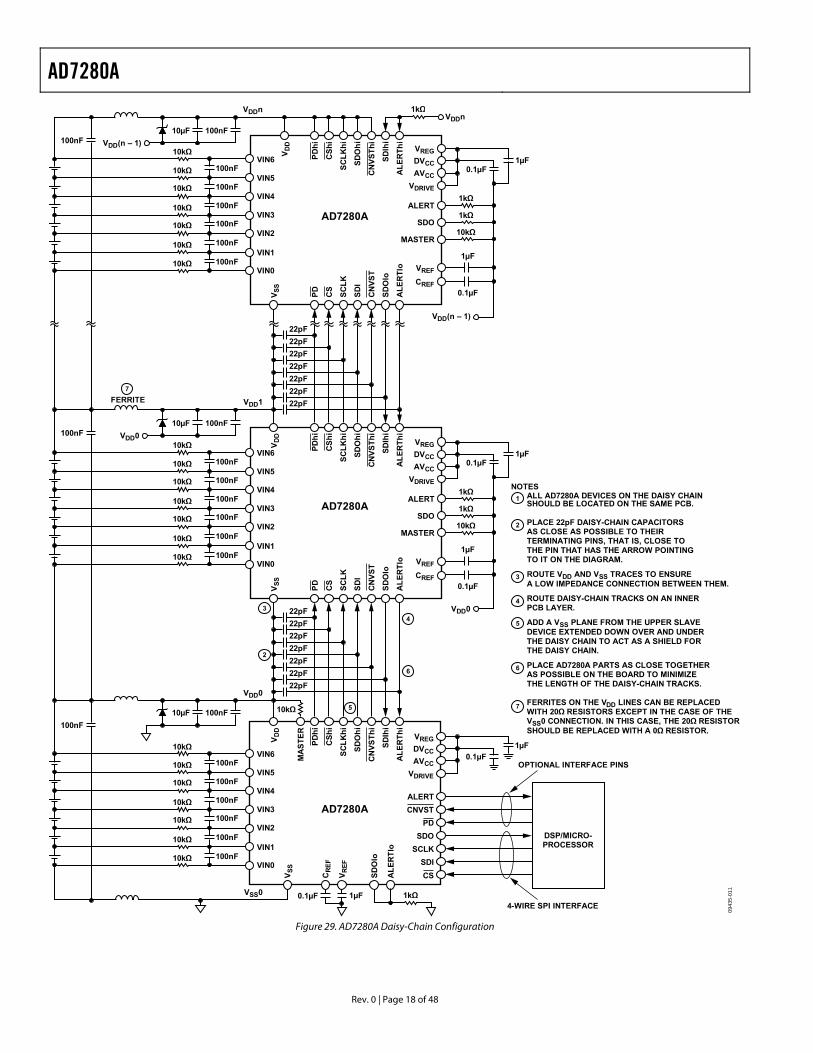
AD7280A
Rev. 0 | Page 18 of 48
VIN6
V DD
V SS
MA
STER
PDhi
CSh
i
SCLK
hi
SDO
hi
CN
VSTh
i
SDIh
i
ALE
RTh
i
V DD
PDhi
CSh
i
SCLK
hi
SDO
hi
CN
VSTh
i
SDIh
i
ALE
RTh
i
PD CS
SCLK
SDI
CN
VST
SDO
lo
ALE
RTl
o
VREG1µF
1µF
0.1µF
0.1µF
VIN5
VIN4
VIN3
VIN2
VIN1
VIN0
V SS
DVCCAVCC
ALERTCNVST
PDSDO
SCLKSDICS
VDRIVE
VREGDVCCAVCC
ALERT
SDO
MASTER
VREF
CREF
VDRIVE
CR
EF
V REF
SDO
lo
ALE
RTl
o
AD7280A
AD7280A
10kΩ
10kΩ
10kΩ
1kΩ
100nF
100nF
10kΩ
10kΩ 100nF
100nF
10kΩ
10kΩ
FERRITE
100nF
10kΩ
100nF
100nF
VIN6
VIN5
VIN4
VIN3
VIN2
VIN1
VIN0
10kΩ
10kΩ 100nF
10kΩ
10kΩ1kΩ
1kΩ
10kΩ
100nF
100nF
10kΩ
10kΩ
100nF
10kΩ
100nF
100nF
100nF10µF
OPTIONAL INTERFACE PINS
4-WIRE SPI INTERFACE
1µF
1µF
0.1µF
0.1µF
22pF22pF22pF22pF22pF22pF22pF
22pF22pF22pF22pF22pF22pF22pF
100nF100nF10µF
VDD0
100nF100nF10µF
VDD(n – 1)
VDDn
VDD1
VDD0
VSS0
VDD0
V SS
V DD
PDhi
CSh
i
SCLK
hi
SDO
hi
CN
VSTh
i
SDIh
i
ALE
RTh
i
PD CS
SCLK
SDI
CN
VST
SDO
lo
ALE
RTl
o
VREGDVCCAVCC
ALERT
SDO
MASTER
VREF
CREF
VDRIVE
VIN6
VIN5
VIN4
VIN3
VIN2
VIN1
VIN0
10kΩ
10kΩ 100nF
10kΩ
10kΩ1kΩ
1kΩ
10kΩ
100nF
100nF
10kΩ
10kΩ
100nF
10kΩ
100nF
100nF
1µF
1µF
0.1µF
0.1µF
VDD(n – 1)
VDDn1kΩ
AD7280A
NOTESALL AD7280A DEVICES ON THE DAISY CHAINSHOULD BE LOCATED ON THE SAME PCB.
PLACE 22pF DAISY-CHAIN CAPACITORSAS CLOSE AS POSSIBLE TO THEIRTERMINATING PINS, THAT IS, CLOSE TOTHE PIN THAT HAS THE ARROW POINTINGTO IT ON THE DIAGRAM.
ROUTE VDD AND VSS TRACES TO ENSUREA LOW IMPEDANCE CONNECTION BETWEEN THEM.
ROUTE DAISY-CHAIN TRACKS ON AN INNERPCB LAYER.
ADD A VSS PLANE FROM THE UPPER SLAVEDEVICE EXTENDED DOWN OVER AND UNDERTHE DAISY CHAIN TO ACT AS A SHIELD FORTHE DAISY CHAIN.
PLACE AD7280A PARTS AS CLOSE TOGETHERAS POSSIBLE ON THE BOARD TO MINIMIZETHE LENGTH OF THE DAISY-CHAIN TRACKS.
FERRITES ON THE VDD LINES CAN BE REPLACEDWITH 20Ω RESISTORS EXCEPT IN THE CASE OF THEVSS0 CONNECTION. IN THIS CASE, THE 20Ω RESISTORSHOULD BE REPLACED WITH A 0Ω RESISTOR.
1
2
3
4
5
6
7
2
34
5
6
7
DSP/MICRO-PROCESSOR
094
35
-01
1
Figure 29. AD7280A Daisy-Chain Configuration

AD7280A
Rev. 0 | Page 19 of 48
REFERENCE The internal reference is temperature compensated to 2.5 V. The reference is trimmed to provide a typical drift of ±3 ppm/°C. As shown in Figure 30, the internal reference circuitry consists of a 1.2 V band gap reference and a reference buffer. The 2.5 V refer-ence is available at the VREF pin. The VREF pin should be decoupled to REFGND using a 1 μF or greater ceramic capacitor. The CREF pin should be decoupled to REFGND using a 0.1 μF or greater ceramic capacitor. The 2.5 V reference is capable of driving an external load of up to 10 kΩ.
VREF
REFGND
CREF
AVCCADC SELF-TESTVOLTAGE
BAND GAP1.2V
09
43
5-0
12
Figure 30. AD7280A Internal Reference
CONVERTING CELL VOLTAGES AND AUXILIARY ADC INPUTS A conversion can be initiated on the AD7280A using either the CNVST input or the serial interface (see the
section). A single conversion command initiates conver-sions on all selected channels of the AD7280A. As described in the section, the voltage of each individual battery cell is measured by converting the difference between adjacent analog inputs. The first cell to be converted following a convert start command is Cell 6, which is the difference between VIN6 and VIN5. At the end of the first conversion, the AD7280A generates an internal end-of-conversion (EOC) signal. This internal EOC selects the next cell voltage inputs for measurement through the multiplexer, that is, the difference between VIN5 and VIN4. The new input is acquired, and a second internal convert start signal is generated, which initiates the conversion. This process is repeated until all the selected voltage and auxiliary ADC inputs have been converted.
Conversion Start Format
Converter Operation
The conversion sequence—that is, the order in which the cell voltages and auxiliary ADC inputs are converted—is shown in Figure 31 and Figure 32. The cell voltage inputs are converted in reverse order, that is, Cell 6 is followed by Cell 5, and so on. However, the auxiliary ADC inputs are converted in increasing numerical order, that is, AUX1 is followed by AUX2, and so on. For example, when all 12 inputs are selected for conversion, the conversion of Cell 1, that is, VIN1 to VIN0, is followed by the conversion of the AUX1 input.
When all selected conversions are completed, the VIN6 and VIN5 voltage inputs are again selected through the multiplexer, and the voltage across Cell 6 is acquired in preparation for the next conversion request. This is the default state for the multiplexer.
Bits[D15:D14] of the control register select the cell voltage and auxiliary ADC inputs to be converted. There are four options available (see Table 8).
Table 8. Cell Voltage and Auxiliary ADC Input Selection Bits[D15:D14] Voltage Inputs Auxiliary ADC Inputs 00 6 to 1 1 to 6 01 6 to 1 1, 3, and 5 10 6 to 1 None 11 ADC self-test None
Each voltage and auxiliary ADC input conversion requires a minimum of 1 μs to acquire and convert the cell voltage or auxiliary ADC input voltage. For example, when Bits[D15:D14] are set to 00, the falling edge of CNVST triggers a series of 12 conversions. This requires a minimum of 12 μs to convert all selected measurements on a single AD7280A. If no auxiliary ADC input conversions are required, Bits[D15:D14] are set to 10. In this case, the conversion request triggers a series of six conversions, requiring a minimum of 6 μs.
t1
tCONV tCONV
tACQ
VOLT 6 VOLT 5 VOLT 4 AUX6INTERNAL ADCCONVERSIONS
CNVST
09
43
5-0
13
Figure 31. ADC Conversions on the AD7280A
t1
tQUIETtWAIT
INTERNAL ADCCONVERSIONS
SERIAL READOPERATION
CNVST
VOLT 6
VOLT4
VOLT 5
VOLT 6 AUX6 VOLT
5
DATA READBACK — ALL DEVICES
CONVERSION WINDOW
09
43
5-0
14
Figure 32. ADC Conversions and Readback on the AD7280A

AD7280A
Rev. 0 | Page 20 of 48
Note that 90 μs should be allowed before initiating any conver-sions following any change to Bits[D15:D14]. This time should be allowed between writing to the control register to change the selected conversions and initiating the first conversion. Conversions that are initiated by the rising edge of the CS pin require two separate write commands to the control register. The first command configures the AD7280A for the required acquisition time; the second command, following a delay of 90 μs, initiates the conversion on the rising edge of CS.
After the completion of all requested conversions, the results can be read back from either a single device or from all devices in a daisy chain by using the SPI and daisy-chain interfaces. For more information, see the Serial Interface section and the Daisy-Chain Interface section.
As shown in Figure 32, a wait time, tWAIT, is required between the completion of conversions and the start of readback. This time is required to synchronize the high speed conversion clock and the lower speed clock used for all other AD7280A operations. The minimum value of tWAIT is 5 μs.
Acquisition Time
The time required to acquire an input signal depends on how quickly the sampling capacitor is charged. This, in turn, depends on the input impedance and any external components placed on the analog inputs. The default acquisition time of the AD7280A on initial power-up is 400 ns. This time can be increased in steps of 400 ns up to 1.6 μs to provide flexibility in selecting external components on the analog inputs. The acquisition time is selected by writing to Bits[D6:D5] in the control register (see Table 9).
Table 9. Analog Input Acquisition Time Bits[D6:D5] Acquisition Time 00 400 ns 01 800 ns 10 1.2 μs 11 1.6 μs
The acquisition time required is calculated using the following formula:
tACQ = 10 × ((RSOURCE + R) × C)
where: RSOURCE should include any extra source impedance on the analog input between the external capacitors (100 nF) and the input pins. It does not include any extra source impedance, for example, the 10 kΩ series resistors, which are between the battery cells and the external capacitors. R is the resistance seen by the track-and-hold amplifier looking at the input, 300 Ω. C is the sampling capacitance, that is, the value of the sampling capacitor, 15 pF.
Conversion Averaging
The AD7280A includes an option where the acquisition and conversion of each cell input can be repeated with an averaged conversion result being stored in the individual register. The averaged conversion result can then be read back through the SPI interface in the same manner as a standard conversion result. The AD7280A can be programmed, through Bits[D10:D9] of the control register, to complete one, two, four, or eight conversions. The default on power-up is a single conversion per channel, that is, no averaging.
Selection of the two, four, or eight average options through the control register causes the control sequence of both the high voltage and low voltage input multiplexers to be reconfigured to allow the additional acquisitions and conversions to be completed. In each case, the requested number of conversions is completed on each channel before beginning the acquisition and conversion of the next channel in sequence. For example, if an average of two conversions is requested, the new sequence is Voltage Channel 6, Voltage Channel 6, Voltage Channel 5, Voltage Channel 5, Voltage Channel 4, and so on.
It should also be noted that when the high voltage multiplexer is reconfigured, 90 μs should be allowed before initiating any conversions. This time should be allowed between writing to the control register to select averaging and initiating the first conversion. Conversions that are being initiated by the rising edge of the CS pin require two separate write commands to the control register. The first command configures the AD7280A for the required averaging, and the second command, after a delay of 90 μs, initiates the conversion on the rising edge of CS.
Suggested External Component Configuration on Analog Inputs
As described in the Acquisition Time section, the acquisition time of the AD7280A is selected by the status of Bits[D6:D5] in the control register. This provides flexibility in selecting external components on the analog inputs. A suggested configuration for placing external components on the analog inputs to the AD7280A is shown in Figure 33.
VIN6
VIN5
VIN4
VIN3
VIN2
VIN1
VIN0
AD7280A10kΩ
10kΩ 100nF
10kΩ
10kΩ 100nF
100nF
10kΩ
10kΩ
100nF
10kΩ
100nF
100nF
094
35
-016
Figure 33. External Series Resistance and Shunt Capacitance

AD7280A
Rev. 0 | Page 21 of 48
The 10 kΩ resistors in series with the inputs provide protection for the analog inputs in the event of an overvoltage or undervoltage on those inputs. The 100 nF capacitor across the differential inputs acts as a low-pass filter in conjunction with the 10 kΩ resistor. The cutoff frequency of the low-pass filter is 80 Hz. Using these external components, the default acquisition time of 400 ns can be used, which allows a combined acquisition and conversion time of 1 μs.
CONVERTING CELL VOLTAGES AND AUXILIARY ADC INPUTS IN A CHAIN OF AD7280As The AD7280A provides a daisy-chain interface that allows up to eight parts to be stacked without the need for individual isola-tion. One feature of the daisy-chain interface is the ability to initiate conversions on all parts in the daisy-chain stack with a single convert start command. The convert start command is transferred up the daisy chain, from the master device to each AD7280A in turn. The delay time between each AD7280A is tDELAY, as shown in Figure 34. The maximum delay between the start of conversions on the master AD7280A and the last AD7280A
device in the chain can be determined by multiplying tDELAY by the number of slave AD7280As in the daisy chain. The total conversion time for all cell voltage and auxiliary ADC input conversions can be calculated using the following equation:
Total Conversion Time = ((tACQ + tCONV) × (Number of Conversions per Part)) − tACQ + ((N − 1) × tDELAY)
where: tACQ is the analog input acquisition time of the AD7280A (see Table 9). tCONV is the conversion time of the AD7280A, as specified in Table 3. Number of Conversions per Part is the number of inputs selected for conversion (6, 9, or 12, as listed in Table 8), multiplied by the number of averages selected for each input (1, 2, 4, or 8). N is the number of AD7280As in the daisy chain. tDELAY is the delay time when transferring the convert start command between adjacent AD7280A devices, as specified in Table 3.
The total conversion times calculated for three possible configurations of the AD7280A are included in Table 10.
tCONV tACQ + tCONV
VOLT 6 VOLT 5
TOTAL CONVERSION TIME =((tACQ + tCONV) × (#CONVERSIONS PER PART)) – tACQ + ((N – 1) × tDELAY)
VOLT 4 AUX6
tDELAY
tDELAY tDELAY
tACQ + tCONV
tDELAY
VOLT 12 VOLT 11 VOLT 10 AUX12
tACQ + tCONV
VOLT 18 VOLT 17 VOLT 16 AUX18
INTERNAL ADCCONVERSIONS
PART 1
SERIAL READOPERATION
PART 2
SERIAL READOPERATION
PART 3
CNVST
094
35
-015
Figure 34. ADC Conversions and Readback on a Chain of Three AD7280As
Table 10. Calculated Conversion Times for Three Example AD7280A Configurations, TA = −40°C to +85°C Bits [D15:D14]
Bits [D10:D9]
Bits [D6:D5] Configuration
Conversion Time per Part
Total Conversion Time per 48 Channel Stack
00 00 00 12 channels; tCONV = 695 ns; tACQ = 465 ns; average = 0 13.46 μs 15.2 μs 01 12 channels; tCONV = 695 ns; tACQ = 1.01 μs; average = 0 19.45 μs 21.2 μs 10 12 channels; tCONV = 695 ns; tACQ = 1.46 μs; average = 0 24.4 μs 26.15 μs 11 12 channels; tCONV = 695 ns; tACQ = 1.89 μs; average = 0 29.13 μs 30.9 μs 10 00 00 6 channels; tCONV = 695 ns; tACQ = 465 ns; average = 0 6.5 μs 8.23 μs 01 6 channels; tCONV = 695 ns; tACQ = 1.01 μs; average = 0 9.22 μs 10.97 μs 10 6 channels; tCONV = 695 ns; tACQ = 1.46 μs; average = 0 11.47 μs 13.22 μs 11 6 channels; tCONV = 695 ns; tACQ = 1.89 μs; average = 0 13.62 μs 15.37 μs 00 11 00 12 channels; tCONV = 695 ns; tACQ = 465 ns; average = 8 110.9 μs 112.65 μs 01 12 channels; tCONV = 695 ns; tACQ = 1.01 μs; average = 8 162.67 μs 164.42 μs 10 12 channels; tCONV = 695 ns; tACQ = 1.46 μs; average = 8 205.42 μs 207.17 μs 11 12 channels; tCONV = 695 ns; tACQ = 1.89 μs; average = 8 246.27 μs 248.02 μs

AD7280A
Rev. 0 | Page 22 of 48
CONVERSION WINDOW As described in the Converting Cell Voltages and Auxiliary ADC Inputs section, the AD7280A converts the selected cell voltage and auxiliary ADC inputs in a defined sequence (see Figure 31). As described in the Circuit Information section, the AD7280A consists primarily of a high voltage input multi-plexer, a low voltage input multiplexer, and a SAR ADC. The six cell voltage channels are presented to the ADC in turn by the high voltage multiplexer. Control is then handed to the low voltage multiplexer that allows the six auxiliary ADC channels to be converted. Following completion of all selected conversions, control is handed back to the high voltage multiplexer, and the AD7280A is ready to receive the next valid convert start command.
The conversion window of the AD7280A includes the actual con-version time for the selected channels (see Table 10), as well as the additional time required to return control to the high voltage multiplexer and configure it to start acquiring the cell voltage between VIN6 and VIN5. The conversion window defines the minimum time that should be allowed between successive convert start commands.
The conversion window for the AD7280A can be calculated using the following equation:
Conversion Window = Total Conversion Time + 80 μs
where Total Conversion Time can be calculated for either a single device or for a chain of devices, as described in the Converting Cell Voltages and Auxiliary ADC Inputs section.
SELF-TEST CONVERSION A self-test conversion can be initiated on the AD7280A, which allows the operation of the ADC and reference buffer to be verified. The self-test conversion is completed on the internal 1.2 V band gap reference voltage, and the voltage range for the conversion is 0 V to 5 V. The self-test conversion can be initi-ated on either a single AD7280A or on all AD7280As in the daisy chain simultaneously.
The conversion results can be read back though the read protocols defined in the Serial Interface section. The self-test conversion result typically varies between Code 970 and Code 990.
The self-test conversion can also be used to verify the operation of the alert outputs, as described in the Alert Output section.
CONNECTION OF FEWER THAN SIX VOLTAGE CELLS The AD7280A provides six input channels for battery cell voltage measurement. The AD7280A can also be used in applications that require fewer than six voltage measurements. In these appli-cations, care should be taken to ensure that the sum of the individual cell voltages still exceeds the minimum VDD supply voltage. For this reason, the recommended minimum number of battery cells connected to each AD7280A is 4. Care should also be taken to ensure that the voltage on the VIN6 input is always greater than or equal to the voltage on the VDD supply pin. For example, in an application with five battery cells connected to the AD7280A, the cell voltage on Cell 5 should be applied across VIN6 and VIN5, and the VIN4 and VIN5 inputs should be shorted together. Figure 35 shows an example of the battery connections to the AD7280A in a four-cell battery monitoring application.
VIN6
VIN5
VIN4
VIN3
VIN2
VIN1
VIN0
AD7280A
10kΩ
10kΩ 100nF
10kΩ
10kΩ
100nF
10kΩ
100nF
100nF
094
35
-017
Figure 35. Typical Connections for a Four-Cell Application
Regardless of how many cell voltage measurements are required in the user application, the AD7280A acquires and converts the voltages on all six cell voltage input channels. The conversion data on all six voltage channels is supplied to the DSP/microprocessor using the SPI/daisy-chain interfaces. Users should ignore the conversion data that is not required in their application.
It is also possible to read back a single cell voltage conversion result from each device in the daisy chain. This can be done by programming the read register on each device to read back the required conversion result (see Example 4 in the Examples of Interfacing with the AD7280A section). However, as previously described, all six cell voltage channels are converted. When using the device in this mode, the overall conversion sample rate should be limited by the conversion window required for the number of channels selected by Bits[D15:D14] of the control register.
When using the alert function, the user should program the alert register to ensure that the shorted channels do not incorrectly trigger an alert output (see the Alert Output section).

AD7280A
Rev. 0 | Page 23 of 48
AUXILIARY ADC INPUTS The AD7280A provides six single-ended analog inputs to the ADC—AUX1 to AUX6—which can be used to convert the voltage output of a thermistor temperature measurement circuit. In the event that no temperature measurements are required or that individual cell temperature measurements are not required, the auxiliary ADC inputs can be used to convert any other 0 V to 5 V input signal.
The AD7280A can be programmed to complete conversions on all six auxiliary ADC channels, on three auxiliary ADC channels (AUX1, AUX3, and AUX5), or on none of the auxiliary ADC input channels. The number of conversions is programmed through Bits[D15:D14] of the control register. The number of conversion results supplied by the AD7280A for readback by the DSP/microprocessor is programmed through Bits[D13:D12] of the control register. It is also possible to read back a single auxiliary ADC conversion result from each device in the daisy chain. This can be done by programming the read register on each device to read back the required conversion result (see Example 4 in the Examples of Interfacing with the AD7280A section). If the device is used in this mode, the overall conversion sample rate should be limited by the conversion window required for the number of channels selected by Bits[D15:D14] of the control register.
In an application where the alert function is used but only one or two auxiliary ADC inputs are required, the AD7280A should first be programmed to complete and read back only three auxiliary ADC conversions by setting Bits[D15:D12] of the control register to 0101. Channel AUX5 and Channel AUX3 can be removed from the alert detection by writing to Bits[D1:D0] of the alert register (see Table 12 in the Alert Output section).
Thermistor Termination Input
If thermistor circuits are used to measure each individual cell temperature, the thermistor termination pin, AUXTERM, can be used to terminate the thermistor inputs for each auxiliary ADC input measurement. This reduces the termination resistor requirement from six resistors to one. Bit D3 in the control register should be set to 1 when using the AUXTERM input.
Note that, due to settling time requirements, the thermistor termi-nation resistor option should only be used when the acquisition time of the AD7280A is set to its highest value (1.6 μs). The acquisition time is configured by setting Bits[D6:D5] of the control register (see Table 9).
In Figure 36, the termination resistor is placed between VSS and AUXTERM. The AUXTERM input can be used to terminate the thermistor inputs to the high or low voltage of the thermistor circuit.
VSS
AUXTERM
RTERM
AUX1
AUX2
AUX3
AUX4
AUX5
AUX6VREG
AD7280A
094
35
-018
Figure 36. Typical Circuit Using the Thermistor Termination Resistor
POWER REQUIREMENTS The current consumed by the AD7280A in normal operation, that is, when not in power-down mode, is dependent on the mode in which the part is being operated. The three distinct modes of operation can be described as follows:
• Voltage and auxiliary ADC input conversion • AD7280A configuration and data readback • Cell balancing
The AD7280A consumes its highest level of current while con-verting voltage and/or auxiliary ADC inputs to digital outputs. Depending on the configuration of the AD7280A, the conversion time can be as little as 6 μs. The typical current required by the AD7280A during conversion is 6.9 mA (see Table 2).
When configuring a chain of AD7280As or when reading back the voltage and/or auxiliary ADC conversion results from a chain of AD7280As, the current required for each AD7280A is typically 6.5 mA (see Table 2). The time required to read back the voltage conversions results from 48 lithium ion cells depends on the speed of the interface clock used, that is, SCLK, but it can be as low as 1.54 ms.
The typical current consumed by the AD7280A when the cell balance outputs are switched on is 6.4 mA (see Table 2). The length of time for which the cell balance outputs are switched on is defined by the user.
When the AD7280A is not being used in any of the aforemen-tioned modes of operation, it is recommended that the device be powered down, as described in the Power-Down section. This significantly reduces the current drawn by each AD7280A in the chain, which avoids unnecessary draining of the lithium ion cells and aids in current matching between devices across the full battery stack.

AD7280A
Rev. 0 | Page 24 of 48
POWER-DOWN The AD7280A provides two power-down options.
• Full power-down (hardware) • Software power-down
Full Power-Down (Hardware)
The AD7280A can be placed into full power-down mode, which requires only 5 μA maximum current, by taking the PD pin low. The falling edge of the PD pin powers down all analog and digital circuitry.
The AD7280A includes a digital delay filter on the PD pin, which protects against a power-down being initiated by noise or glitches on the hardware PD pin. A hardware power-down is not initiated until the PD pin is held low for approximately 130 μs. Similarly, the AD7280A is not taken out of power-down mode until the PD pin is held high for approximately 130 μs. The digital delay filter does not apply on initial power-up. The power-on request is accepted by the AD7280A approximately 5 μs after the rising edge of PD.
When placing the AD7280A into full power-down mode, AVCC and DVCC must fall to 0 V and must not be held high by any external means. AVCC and DVCC can be held high unintention-ally if the auxiliary ADC inputs are greater than the forward bias on the internal ESD protection diodes. For this reason, it is recommended that the auxiliary ADC inputs return to 0 V when the part is placed in full power-down mode.
In addition, all digital inputs on the AD7280A master device must return to 0 V when the part is placed in full power-down mode (see Figure 37). However, if an external VDRIVE supply is used—that is, VDRIVE is not connected to VREG—then only the CNVST line must return low (see ). Figure 38
When the AD7280A is placed into full power-down mode, the device must be left in full power-down for a minimum of 2 ms when the VREG and VREF pins are decoupled with 1 μF capacitors. This ensures that the charge on the VREG and VREF decoupling capacitors dissipates sufficiently to allow the internal power-on reset circuit to activate when powering the AD7280A back up.
This time is measured from the falling edge of the PD pin. shows a plot of the voltage on the VREG and VREF pins
as the AD7280A is powering down with 1 μF decoupling capacitors on the pins. shows a similar plot but with 10 μF decoupling capacitors on the VREG and VREF pins.
Figure 18
Figure 20
VSS
AD7280A
VREG
0.1µF 10µF
1µF
0.1µF
0.1µF
VDD
VDD
DVCC
AVCC
1µF
0.1µF
VREF
CREF
ALERTSDO
SCLKSDI
VDRIVE
MASTER
AUX6AUXTERM
AUX5AUX4AUX3AUX2AUX1
10kΩ
MUST GO TO 0V INHARDWARE POWER-DOWN
MUST GO TO 0VIN HARDWAREPOWER-DOWN
CSPD
CNVST
DSP/MICRO-PROCESSOR
09
43
5-0
23
Figure 37. VDRIVE Powered from VREG
VSS
AD7280A
VREG
0.1µF 10µF
1µF
0.1µF
0.1µF
VDD
VDD
10µF0.1µF
DVCC
AVCC
1µF
0.1µF
VREF
CREF
ALERTSDO
SCLKSDI
VDRIVE
MASTER
AUX6AUXTERM
AUX5AUX4AUX3AUX2AUX1
10kΩ
MUST GO TO 0V INHARDWARE POWER-DOWN
MUST GO TO 0VIN HARDWAREPOWER-DOWN
CSPD
CNVST
DSP/MICRO-PROCESSOR
2.7V TO 5.5V SUPPLY
09
43
5-0
24
Figure 38. VDRIVE Powered from DSP/Microprocessor

AD7280A
Rev. 0 | Page 25 of 48
Software Power-Down
The AD7280A can be placed into software power-down mode, which requires 3.8 mA of current, by setting Bit D8 in the control register through the serial interface. The CNVST pin should be gated out before generating a software power-down (see the CNVST Control Register section). When the AD7280A is powered down through the serial interface, the regulator, the reference, and the daisy-chain circuitry stay powered up, but the remaining analog and digital circuitry is powered down. This is necessary to ensure that the signal to power on the part, or the chain of parts, is correctly received.
Power-Down Timer
The PD timer register allows the user to program a set time after which the AD7280A is automatically powered down. This timer functions as a time delay between the falling edge of the PD input (or the setting of Bit D8 in the control register) and the AD7280A powering down. The PD timer can be set to a value from 0 minutes to 36.9 minutes, with a resolution of 71.5 sec. The user should first write to the PD timer register to define the desired delay. Any subsequent falling edge on the PD input or setting of Bit D8 in the control register starts the PD timer. When the programmed time elapses, the AD7280A checks the state of the PD pin. If the PD pin is low, the AD7280A powers down. If the PD pin is high, the part does not power down and continues to operate as normal. The default value of the PD timer register on power-up is 0x00.
If the PD timer register is written to after the counter starts, the counter is reset to 0. The count then restarts automatically, without further input from the user, and counts to the new value in the PD timer register. If the new time in the PD timer register is 0, the part checks the state of the PD pin and powers down if the PD pin is low. Note that when the PD timer is activated—for example, by a falling edge on the PD pin—a subsequent rising edge on the PD pin does not disable the active PD timer. It is recommended that the PD pin be held low until an active PD timer expires.
POWER-UP TIME As described in the Power-Down section, a full power-down of the AD7280A (active low on the PD input) powers down all analog and digital circuitry. The recommended power-up time from hardware power-down, when the internal reference is decoupled with a 1 μF capacitor, is 5.5 ms. It is recommended that no conversions be initiated until the 5.5 ms power-up time elapses because such conversions can result in inaccurate data.
A software power-down powers down all analog and digital circuitry on the AD7280A except for the regulator, the 1.2 V band gap reference, and the daisy-chain circuitry. The recom-mended power-up time from software power-down, when the VREF pin is decoupled with a 1 μF capacitor, is 1 ms.
CELL BALANCING OUTPUTS The AD7280A provides six cell balance outputs that can be used to drive the gate of external transistors as part of a cell balancing circuit. Each CBx output can be set to provide either a 0 V or 5 V output with respect to the absolute amplitude of the negative terminal of the battery cell that is being balanced. For example, the CB6 output provides a 0 V or 5 V output with respect to the voltage on the VIN5 analog input. The CBx outputs are set by writing to the cell balance register. The default value of the cell balance register on power-up is 0x00.
VIN6
CB6
VIN5
CB5
VIN4
CB4
VIN3
CB3
VIN2
CB2
VIN1
CB1
VIN0
AD7280A
10kΩ
10kΩ
10kΩ
10kΩ
10kΩ
10kΩ
09
43
5-0
19
Figure 39. Cell Balancing Configuration
As noted in the Power-Down Timer section, a power-down timer can be programmed on the AD7280A. This timer can be used to allow cell balancing to occur for a set time before powering down the AD7280A. The power-down timer is independent of the cell balance timers. If no power-down timer is set—that is, if the PD timer register is at its default value of 0x00—a falling edge on the PD pin switches off the CBx outputs and powers down the AD7280A. If a power-down timer is set, the CBx outputs are powered down when the programmed power-down timer elapses and the AD7280A is powered down.
In an application with two or more AD7280A devices in a daisy chain, it is recommended that series resistors be placed between the CBx outputs of the AD7280A and the gates of the external cell balancing transistors. These resistors are recommended to protect the AD7280A in the event that the external cell balancing transistors are damaged during the initial connection of the monitoring circuitry to the battery stack. Consideration should also be given to the protection of these external transistors during the initial connection of the monitoring circuitry to the battery stack.
AD7280A
Rev. 0 | Page 26 of 48
An example of how damage to the external transistors can occur is a connection sequence that first provides the system ground (the ground supply to the master AD7280A in the daisy chain) followed by a connection from any of the battery cells at a potential high enough to exceed the VGS of the cell balancing transistor, for example 40 V. If these two connections are the first battery connections made in the system, the result is 40 V being applied to one of the VINx pins of the AD7280A through a series resistor. The 40 V battery connection is also directly applied to the source input of one of the cell balancing transistors. However, because no power has been supplied to the VDD pin of the AD7280A, all the CBx outputs are at 0 V. This results in a reverse voltage of 40 V across the VGS of the external transistor, which can damage the device.
Cell Balance Timers
The AD7280A offers six cell balance timer registers that allow the on time of each CBx output to be programmed. The CBx timers can be set to a value from 0 minutes to 36.9 minutes. The resolution of the CBx timers is 71.5 sec. A value of 0x00 in a CBx timer register means that the timer is not activated. A non-zero value programmed to a CBx timer register configures the CBx timer for use, but the CBx outputs and the CBx timers are not activated until the cell balance register is written to. At the end of the individually programmed CBx time, the respective CBx output returns to its default state of 0 V output with respect to the absolute amplitude of the negative terminal of the battery cell that is being balanced. Also at this time, the cell balance register is reset and the CBx timer registers continue to hold their programmed values. The default value of the CBx timer registers on power-up is 0x00.
When using the cell balance timer feature, note that the timer on each cell balance output is operated from a single CB counter. When a nonzero value is programmed to any CBx timer register, this counter is activated by writing a nonzero value to the cell balance register. The current value of the counter is compared to the values programmed to each CBx timer register at 4.5 sec intervals (71.5 sec/16). When the value in the counter reaches the value in the CBx timer register, the cell balance output corresponding to that CBx timer register is switched off. Note that the cell balance register has a higher priority than the CBx timer registers. A CBx output can be switched off by writing to the cell balance register even if the value programmed to the respective CBx timer register has not expired.
Writing a zero or a nonzero value to an active CBx timer register (corresponding CB output switched on) results in the cell balance counter being reset and automatically restarted. Note that overwriting the CBx timer with 0 restarts the counter, but, because the timer value is now 0, the corresponding CB output is switched off. Any write to a nonactive CBx timer register (corresponding CB output not switched on) has no effect on the cell balance counter.
Programming the Cell Balance Timers
It is recommended that the required CBx timer values be programmed to each individual CBx timer register before activating the CB counter. Changing the CBx timer values while the counter is running is possible; however, writing to an active CBx timer register resets the counter, as described in the Cell Balance Timers section.
Cell Balance Timer Example 1
The following sequence of steps programs a value of 214.5 sec to the CB1 and CB2 timer registers.
1. Set Bits[D4:D3] of the CB1 timer register and the CB2 timer register high.
2. Set Bits[D3:D2] of the cell balance register high. 3. Wait 60 sec. 4. Set Bits[D4:D3] of the CB3 timer register high. 5. Set Bits[D4:D2] of the cell balance register high.
In this example, the CB1 and CB2 outputs are switched on and the cell balance counter is activated. Following the 60 sec wait, a value of 214.5 sec is written to the CB3 timer register, the CB3 output is switched on, and the on state of the CB1 and CB2 outputs is maintained. In this example, all three CB outputs are switched off at the same time (214.5 sec). This is because the CB counter was already active before the CB3 timer register was programmed and the CB3 output selected.
Cell Balance Timer Example 2
In this example, follow the same sequence of steps described in the Cell Balance Timer Example 1 section, but increase the wait step from 60 sec to any value greater than 214.5 sec.
The initial steps set up the CB1 and CB2 timers and activate the CB1 and CB2 outputs. However, because the wait state is now longer than the time programmed to the CB1 and CB2 timers, the CB1 and CB2 timers expire before the additional writes to configure CB3. The CB1 and CB2 outputs switch off, a 0 is written to Bits[D3:D2] of the cell balance register, and the CB counter is reset to 0x00 before the commands to program the CB3 timer and to switch on the CB3 output are received.
In this example, the second write to the cell balance registers—which selects the CB1, CB2, and CB3 outputs—is considered a new activation of the CB counter. The CB1, CB2, and CB3 outputs switch on and, if no further commands are written to the AD7280A, all three outputs switch off 214.5 sec after this second activation of the CB counter.

AD7280A
Rev. 0 | Page 27 of 48
ALERT OUTPUT The alert output on the AD7280A can be used to indicate whether any of the following faults has occurred:
• Cell overvoltage • Cell undervoltage • Auxiliary ADC overvoltage • Auxiliary ADC undervoltage
Following each completed conversion, the cell voltage and auxiliary ADC measurement results are compared to the alert thresholds. The alert thresholds are set by writing to the cell overvoltage, cell undervoltage, AUX ADC overvoltage, and AUX ADC undervoltage registers. An alert output is generated if the cell voltage and/or the auxiliary ADC results are outside the programmed alert thresholds.
The alert output can be configured as a static or dynamic output by writing to the alert register. The static alert output is a high signal that is pulled low in the event of an overvoltage or under-voltage on the cell voltage or auxiliary ADC input conversions. The dynamic alert is a square wave that can be programmed to a frequency of 100 Hz, 1 kHz, or 10 kHz. The alert output can be used as part of a daisy chain, in which case the AD7280A at the top of the chain, that is, farthest away from the DSP/micro-processor, should be programmed to generate the initial alert output, and all other devices in the chain should be programmed to allow the alert signal to pass through. If a conversion result outside the programmed thresholds occurs, either on the device generating the initial alert signal or on any device in the chain, the alert signal is pulled low to indicate that an alert condition has occurred. At the end of the daisy chain, the master AD7280A, which is connected to the DSP/microprocessor, takes the alert signal from the chain and passes it in standard digital voltage format to the DSP/microprocessor. The configuration settings for the alert register are described in Table 11 and Table 12.
Table 11. Alert Register Settings, Bits[D7:D4]1 Bits[D7:D6] Bits[D5:D4] Action 00 XX No alert signal generated or
passed (default) 01 XX Generates a static (high) alert
signal to be passed down the daisy chain
10 00 Generates a 100 Hz square wave alert signal to be passed down the daisy chain
10 01 Generates a 1 kHz square wave alert signal to be passed down the daisy chain
10 10 Generates a 10 kHz square wave alert signal to be passed down the daisy chain
10 11 Reserved 11 XX Passes an alert signal from the
AD7280A at higher potential in the daisy chain
1 X is don’t care.
Table 12. Alert Register Settings, Bits[D3:D0]1 Bits[D3:D2] Bits[D1:D0] Action 00 XX Includes all six voltage channels in
alert detection (default) 01 XX Removes VIN5 from alert
detection 10 XX Removes VIN5 and VIN4 from alert
detection 11 XX Reserved XX 00 Includes all AUX ADC channels
selected for conversion in alert detection2 (default)
XX 01 Removes AUX5 from alert detection3
XX 10 Removes AUX5 and AUX3 from alert detection3
XX 11 Reserved
1 X is don’t care. 2 Includes six auxiliary ADC channels in the alert detection if conversions on
six auxiliary ADC channels are selected in the control register; includes three auxiliary ADC channels in the alert detection if conversions on three auxiliary ADC channels are selected in the control register.
3 To remove AUX5 or AUX5 and AUX3 from the alert detection, conversions on three auxiliary ADC input channels only must be selected in the control register.
Some applications require fewer than six voltage measurements (see the Connection of Fewer Than Six Voltage Cells section). As shown in Figure 35, it is recommended that a channel that is not being used on the AD7280A be shorted to the channel below it. To prevent the incorrect triggering of the alert output in this application, the AD7280A allows the user to select up to two voltage channels that can be taken out of the overvoltage/ undervoltage detection circuit. This is programmed through Bits[D3:D2] of the alert register. The user can also remove all or selected auxiliary ADC channels from the detection circuit. This is programmed through Bits[D1:D0] of the alert register in combination with Bits[D15:D14] of the control register.
The operation of the alert output can be verified by initiating a self-test conversion. The self-test conversion converts the band gap reference voltage, 1.2 V, which triggers an alert output if the cell undervoltage threshold is set higher than 1.2 V. To test the alert output, a self-test conversion should be initiated on the AD7280A farthest away from the DSP/microprocessor.
The operation of the alert output can also be verified by increas-ing or decreasing the thresholds around a known input voltage to trigger an alert condition. The alert operation of each device in the daisy chain of AD7280As can be verified by, for example, decreasing the cell overvoltage threshold of that device below the value of the input voltage on the cells. Initiating a conversion on all devices in the daisy chain pulls the alert signal low as it passes through that device. The relevant threshold on that device can then be returned to its previous value and the process repeated on the next device in the daisy chain.

AD7280A
Rev. 0 | Page 28 of 48
REGISTER MAP Table 13.
Register Name Register Address
Register Data
Read/Write Register
Cell Voltage 1 0x00 D11 to D0 Read only Cell Voltage 2 0x01 D11 to D0 Read only Cell Voltage 3 0x02 D11 to D0 Read only Cell Voltage 4 0x03 D11 to D0 Read only Cell Voltage 5 0x04 D11 to D0 Read only Cell Voltage 6 0x05 D11 to D0 Read only AUX ADC 1 0x06 D11 to D0 Read only AUX ADC 2 0x07 D11 to D0 Read only AUX ADC 3 0x08 D11 to D0 Read only AUX ADC 4 0x09 D11 to D0 Read only AUX ADC 5 0x0A D11 to D0 Read only AUX ADC 6 0x0B D11 to D0 Read only Self-Test 0x0C D11 to D0 Read only Control 0x0D D15 to D8 Read/write 0x0E D7 to D0 Read/write Cell Overvoltage 0x0F D7 to D0 Read/write Cell Undervoltage 0x10 D7 to D0 Read/write AUX ADC Overvoltage 0x11 D7 to D0 Read/write AUX ADC Undervoltage 0x12 D7 to D0 Read/write Alert 0x13 D7 to D0 Read/write Cell Balance 0x14 D7 to D0 Read/write CB1 Timer 0x15 D7 to D0 Read/write CB2 Timer 0x16 D7 to D0 Read/write CB3 Timer 0x17 D7 to D0 Read/write CB4 Timer 0x18 D7 to D0 Read/write CB5 Timer 0x19 D7 to D0 Read/write CB6 Timer 0x1A D7 to D0 Read/write PD Timer 0x1B D7 to D0 Read/write Read 0x1C D7 to D0 Read/write CNVST Control 0x1D D7 to D0 Read/write
CELL VOLTAGE REGISTERS The cell voltage registers store the conversion result from each cell input. The conversion result is in 12-bit straight binary format.
AUXILIARY ADC REGISTERS The AUX ADC registers store the conversion result from each auxiliary ADC input. The conversion result is in 12-bit straight binary format.
SELF-TEST REGISTER The self-test register stores the conversion result of the ADC self-test. The conversion result is in 12-bit straight binary format.
CONTROL REGISTER The control register is a 16-bit register that is used to configure the AD7280A. Table 14 describes the operation of each bit in the control register.
Table 14. Control Register Settings Bits Description [D15:D14] Select conversion inputs 00 = six cell voltages and six AUX ADCs (default) 01 = six cell voltages and AUX1, AUX3, and AUX5 10 = six cell voltages only 11 = ADC self-test [D13:D12] Read conversion results 00 = six voltages and six AUX ADCs (default) 01 = six voltages and AUX1, AUX3, and AUX5 10 = six cell voltages only 11 = no-read operation D11 Conversion start format 0 = falling edge of CNVST input (default)
1 = rising edge of CS
[D10:D9] Conversion averaging 00 = single conversion only (default) 01 = average by 2 10 = average by 4 11 = average by 8 D8 Power-down format 0 = falling edge of PD input (default)
1 = software power-down D7 Software reset 0 = take the AD7280A out of reset (default) 1 = reset the AD7280A [D6:D5] Set acquisition time 00 = 400 ns (default) 01 = 800 ns 10 = 1.2 μs 11 = 1.6 μs D4 Reserved; set to 1 D3 Thermistor termination resistor 0 = function not in use (default) 1 = termination resistor connected D2 Lock device address 0 = does not lock to new device address; continues
to operate with Device Address 0x00 (default) 1 = part locks to new device address that it is
presented with D1 Increment device address 0 = does not increment the device address when
transferring data up the daisy chain 1 = increments the device address when
transferring data up the daisy chain (default) D0 Daisy-chain register readback 0 = function not in use; registers are read in single
register readback mode 1 = set daisy chain for register readback (default)

AD7280A
Rev. 0 | Page 29 of 48
Select Conversion Inputs
Bits[D15:D14] of the control register determine which cell voltages and auxiliary ADC inputs are converted following a convert start command. The default value of D15 and D14 on power-up is 00.
Read Conversion Results
Bits[D13:D12] of the control register determine which cell voltage and auxiliary ADC conversion results are supplied to the serial or daisy-chain data output pins for readback. The default value of D13 and D12 on power-up is 00.
Conversion Start Format
A conversion on the AD7280A can be initiated through the hardware CNVST pin or by issuing a software convert start command. Bit D11 of the control register determines whether a conversion is initiated on the falling edge of the CNVST input or on the rising edge of the CS input. The default format on power-up is the CNVST pin, that is, 0. When using the rising edge of the CS input to initiate conversions, Bit D11 is reset to 0 following the initiation of conversions.
Conversion Averaging
Bits[D10:D9] of the control register determine the number of conversions completed on each input with the averaged results stored in the relevant result registers. The user can select a single conversion only or the average of two, four, or eight conversions. The default value of Bits[D10:D9] on power-up is 00, that is, single conversion only.
Power-Down Format
Setting Bit D8 of the control register places the AD7280A into software power-down. See the Power-Down section for more information. The default value of Bit D8 on power-up is 0.
Software Reset
Bit D7 of the control register allows the user to initiate a software reset of the AD7280A. Two write commands are required to complete the reset operation. Bit D7 must be set high to put the AD7280A into reset. Bit D7 must then be set low to take the AD7280A out of reset. A software reset resets all user configurable registers to their default values with the exception of the lower byte of the control register (Address 0x0E). When executing a software reset, care should be taken to ensure that Bits[D6:D0] are not incorrectly overwritten.
Set Acquisition Time
Bits[D6:D5] of the control register determine the acquisition time of the ADC. See the Acquisition Time section for more information. The default value of the acquisition time is 400 ns, that is, 00.
Thermistor Termination Resistor
Bit D3 of the control register should be set if the user wishes to use a single thermistor termination resistor on the AUXTERM pin. Note that, due to settling time requirements, the thermistor termination resistor option should only be used when the acqui-sition time of the AD7280A is set to its highest value, that is, 1.6 μs (set Bits[D6:D5] to 11). The default value of D3 is 0.
Lock Device Address
Bit D2 of the control register is used in conjunction with Bit D1 to allow individual device addresses for each AD7280A in the daisy chain to be defined and locked to the part. Bit D1 is used to generate the individual device addresses that are presented to each AD7280A in the daisy chain in the form of a write command. When Bit D2 is set high, the AD7280A locks to the device address presented to it. This new device address is used for all subsequent CRC calculations. When Bit D2 is set low, the device address of the AD7280A is not locked. In this case, a device address of 0x00 is used for CRC calculations. The default value of D2 is 0.
Increment Device Address
Bit D1 of the control register determines whether the AD7280A increments the device address that it receives as part of a write command when transferring that command up the daisy chain. When Bit D1 is set to 1, the device address is incremented as the command is passed up the chain. This mode of operation is used on initial power-up and when coming out of a hardware power-down to allow individual device addresses for each AD7280A in the daisy-chain stack to be defined. When D1 is set low, no change is made to the device address as the command is passed up the chain. The default value of D1 is 1.
Daisy-Chain Register Readback
Bit D0 of the control register enables the readback of individual registers from each AD7280A in a daisy chain. When Bit D0 is set high, the application of sufficient clocks allows the data stored in the register address identified by the read register to be shifted out of each AD7280A in turn. This data is passed down the daisy chain and read back by the DSP/microprocessor. When Bit D0 is set low, daisy-chain read is disabled. See the Daisy-Chain Interface section and the Examples of Interfacing with the AD7280A section. The default value of D0 is 1.
CELL OVERVOLTAGE REGISTER The cell overvoltage register determines the high voltage thresh-old of the AD7280A. Cell voltage conversions that exceed the overvoltage threshold trigger the alert output. The AD7280A allows the user to set the overvoltage threshold to a value from 1 V to 5 V. The resolution of the overvoltage threshold is eight bits, that is, 16 mV. The default value of the overvoltage threshold on power-up is 0xFF (5 V).

AD7280A
Rev. 0 | Page 30 of 48
CELL UNDERVOLTAGE REGISTER The cell undervoltage register determines the low voltage thresh-old of the AD7280A. Cell voltage conversions lower than the undervoltage threshold trigger the alert output. The AD7280A allows the user to set the undervoltage threshold to a value from 1 V to 5 V. The resolution of the undervoltage threshold is eight bits, that is, 16 mV. The default value of the undervoltage threshold on power-up is 0x00 (1 V).
AUX ADC OVERVOLTAGE REGISTER The AUX ADC overvoltage register determines the high voltage threshold of the AD7280A auxiliary ADC inputs. Conversions that exceed this threshold trigger the alert output. The AD7280A allows the user to set the threshold to a value from 0 V to 5 V. The resolution is eight bits, that is, 19 mV. The default value of the auxiliary ADC overvoltage threshold on power-up is 0xFF (5 V).
AUX ADC UNDERVOLTAGE REGISTER The AUX ADC undervoltage register determines the low voltage threshold of the AD7280A auxiliary ADC inputs. Conversions that are lower than this threshold trigger the alert output. The AD7280A allows the user to set the threshold to a value from 0 V to 5 V. The resolution is eight bits, that is, 19 mV. The default value of the AUX ADC undervoltage threshold on power-up is 0x00 (0 V).
ALERT REGISTER The alert register determines the configuration of the alert function. The alert can be configured as a static or dynamic signal.
• The static signal is a high signal that is pulled low to indicate that an overvoltage or undervoltage on a cell or on the auxiliary ADC has occurred.
• The dynamic signal is a square wave, the frequency of which can be set to 100 Hz, 1 kHz, or 10 kHz.
When a number of AD7280As are operating in daisy-chain mode, the selection of static or dynamic alert is set on the AD7280A at the highest potential in the chain only. The alert registers on the remaining AD7280As in the chain should be programmed to pass the alert signal through the chain. Each part passes the static or dynamic alert signal through the chain or pulls the signal low to indicate that an overvoltage or under-voltage on a cell or on the auxiliary ADC has occurred.
See Table 11 and Table 12 for more information about the alert register settings. The default value of the alert register on power-up is 0x00.
CELL BALANCE REGISTER The cell balance register determines the status of the six cell balance outputs. The six CBx outputs are set by writing to Bits[D7:D2] of the cell balance register. The cell balance register is reset by a software reset or following a hardware power-down. The default value of the cell balance register on power-up is 0x00.
Table 15. Cell Balance Register Settings Bits Description D7 Set CB6 output 0 = output off 1 = output on D6 Set CB5 output 0 = output off 1 = output on D5 Set CB4 output 0 = output off 1 = output on D4 Set CB3 output 0 = output off 1 = output on D3 Set CB2 output 0 = output off 1 = output on D2 Set CB1 output 0 = output off 1 = output on [D1:D0] Reserved; set to 0
CBx TIMER REGISTERS The CBx timer registers allow the user to program individual times for each cell balance output. The AD7280A allows the user to set the CBx timer to a value from 0 minutes to 36.9 minutes. The resolution of the CBx timers is 71.5 sec. The default value of the CBx timer registers on power-up is 0x00. When the CBx timer value is set to 0x00, the CBx timer is not activated; that is, the CBx outputs are all controlled by the contents of the cell balance register only. For more information, see the Cell Balancing Outputs section.
Table 16. CBx Timer Register Settings Bits Description [D7:D3] 5-bit binary code to set the CB timer to a value
from 0 minutes to 36.9 minutes [D2:D0] Reserved; set to 000

AD7280A
Rev. 0 | Page 31 of 48
PD TIMER REGISTER The PD timer register allows the user to configure a set time after which the AD7280A is automatically powered down. The AD7280A allows the user to set the PD timer to a value from 0 minutes to 36.9 minutes. The resolution of the PD timer is 71.5 sec. When using the PD timer in conjunction with the CBx timers, the value programmed to the PD timer should exceed that programmed to the CBx timer by at least 71.5 sec because the PD timer takes priority over the CBx timers. The default value of the PD timer register on power-up is 0x00.
Table 17. PD Timer Register Settings Bits Description [D7:D3] 5-bit binary code to set the PD timer to a value
from 0 minutes to 36.9 minutes [D2:D0] Reserved; set to 000
READ REGISTER The read register, in conjunction with Bits[D13:D12] and Bit D0 of the control register, defines the read operations of the AD7280A. To read back a single register from either a single AD7280A or from a chain of AD7280A devices, the desired register address should first be written to the read register. To read back a series of conversion results from either a single AD7280A or from a chain of AD7280A devices, an address of 0x00 should be written to the read register. The default value of the read register on power-up is 0x00.
Table 18. Read Register Settings Bits Description [D7:D2] 6-bit binary address for the register to be read [D1:D0] Reserved; set to 00
CNVST CONTROL REGISTER
The CNVST control register allows the user to gate the input signal from the CNVST pin.
Bit D0 of the CNVST control register allows the user to hold the internal CNVST signal high regardless of any external noise or glitches on the CNVST pin. This setting can be used in noisy environments to prevent incorrect initiation of conversions. When using the rising edge of CS to perform a software convert start, it is recommended that the CNVST pin be gated out by setting Bit D0 high (see the section). Conversion Start Format
Bit D1 of the CNVST control register allows the user to open a window in the CNVST gate that allows a single CNVST pulse through. The window is closed automatically following a falling edge on the CNVST pin. To use this functionality, the user should write 10 to Bits[D1:D0] of the CNVST control register immediately before each conversion start request.
The default value of the CNVST control register on power-up is 0x00.
Table 19. CNVST Control Register Settings Bits [D7:D2]
Bit D1
Bit D0 Description
000000 0 0 CNVST input not gated (default).
000000 X 1 CNVST input gated.
000000 1 0 Allow single CNVST pulse. Additional CNVST pulses are gated.
AD7280A
Rev. 0 | Page 32 of 48
SERIAL INTERFACE The AD7280A serial interface is Mode 1 SPI compliant, that is, the clock polarity (CPOL) is 0, and the clock phase (CPHA) is 1. The interface consists of four signals: CS, SCLK, SDI, and SDO. The SDI line is used to transfer data into the on-chip registers, and the SDO line is used to read the on-chip registers and conversion result registers. SCLK is the serial clock input for the device; all data transfers, either on SDI or on SDO, take place with respect to SCLK. Data is clocked into the AD7280A on the SCLK falling edge. Data is clocked out of the AD7280A on the SCLK rising edge. The CS input is used to frame the serial data being transferred to or from the device.
The AD7280A allows 32-bit data transfer only and resets a counter on the rising edge of CS to ensure that the AD7280A is automatically resynchronized with the DSP/microprocessor on every falling edge of CS. Individual 8-bit or 16-bit words can be used to assemble a 32-bit command, but a single 32-bit wide CS frame is required to correctly structure the assembly of the 32-bit command.
The rising edge of CS can also be used to initiate the sequence of conversions by writing to the upper byte of the control register.
shows the timing diagram for the serial interface of the AD7280A. See the section for more information about the daisy-chain interface.
Figure 2Daisy-Chain Interface
WRITING TO THE AD7280A In a battery monitoring application, up to eight AD7280As can be daisy-chained to allow up to 48 individual Li-Ion cell voltages to be monitored. Each write operation must, therefore, include a device address and a register address, in addition to the data to be written. An additional identifier bit is also required when addressing all AD7280As in the daisy chain. The AD7280A SPI interface, in combination with the daisy-chain interface, allows any register in the stack of eight AD7280As to be updated using one 32-bit write cycle. The 32-bit write sequence is shown in Table 20. The AD7280A also requires an 8-bit CRC to be included in each write command.
Device Address
The device address is a 5-bit address that allows each individual AD7280A in the battery monitoring stack to be uniquely identified. On initial power-up, each AD7280A is configured with a default address of 0x00. A simple sequence of commands allows each AD7280A to recognize its unique device address in the stack (see the Initializing the AD7280A section).
This device address can then be locked to the AD7280A and used in subsequent read and write commands. The device address is written to and read from the AD7280A stack in reverse order, that is, LSB first.
Register Address
The register map for the AD7280A is provided in Table 13. Each register address is six bits long and is used when writing to or reading from the on-chip registers of the AD7280A.
Register Data
When issuing a write command to a part in the stack of AD7280A devices, the data to be written is an 8-bit word. As shown in Table 13, all read/write registers are eight bits wide. For more information about the correct settings for each register, see the Register Map section.
Address All Parts
The AD7280A allows write commands to be issued simultane-ously to all devices in the daisy chain, as well as write commands to individual AD7280As. A write to all devices in the daisy chain is completed by setting Bit D12 of the write command to 1. When issuing a write all command, the device address should be set to 0x00. This device address is also used to calculate the 8-bit CRC for transmission with the write all command.
8-Bit CRC
The AD7280A includes an 8-bit cyclic redundancy check (CRC) on all write commands to either individual devices or to a chain of devices. An AD7280A that receives an invalid CRC in the write command does not execute the command. The CRC on the write command is calculated based on Bits[D31:D11] of the write command. These bits include the device address, the register address, the data to be written, the address all parts bit, and Bit D11. For more information about the CRC, see the Cyclic Redundancy Check section.
Bit Pattern (010)
A required fixed bit pattern of 010 to Bits[D2:D0] of the 32-bit write command of the AD7280A provides an additional stage of verification. The correct position of this bit pattern is verified on each write command received by the AD7280A. An AD7280A that receives an incorrect bit pattern in the write command does not execute the command.
Table 20. 32-Bit Write Cycle Device Address1 Register Address Register Data Address All Parts Reserved (0 Bit) 8-Bit CRC Bit Pattern (010) D31 to D27 D26 to D21 D20 to D13 D12 D11 D10 to D3 D2 to D0 1 The device address is configured LSB first. For example, to address the second device in the stack, that is, the first slave device, the sequence of bits input to the
AD7280A should be 10000. The register address, data bits, and CRC bits are input MSB first.

AD7280A
Rev. 0 | Page 33 of 48
READING FROM THE AD7280A There are two types of read operation for the AD7280A:
• Conversion results read • Register data read
The data returned from a conversion result read operation includes the device address, the channel address, the write acknowledge bit, and the 8-bit CRC information, in addition to the 12 bits of conversion data. Table 21 illustrates the 32-bit read cycle for a conversion result read.
The data returned from a register data read operation includes the device address, the register address, the write acknowledge bit, and the 8-bit CRC information, in addition to the eight bits of register data. Table 22 illustrates the 32-bit read cycle for a register data read.
The AD7280A SPI interface, in combination with the daisy-chain interface, allows the conversion results of any AD7280A in a stack of eight AD7280As to be read back using an N × 8 × 32-bit read cycle, where N is defined as the number of conver-sions completed on that part, that is, 12, 9, or 6 (see Table 8).
Device Address
The device address is described in the Writing to the AD7280A section. When reading back register or conversion data from the device using the daisy-chain readback mode, the SDI line must be set to write to a specific address. That is, the SDI line should not be allowed to idle high or low, and the address all parts bit must be set to 0. The address must be either the top part in the chain of AD7280A devices or an address with a value higher than that of the top part in the chain. Writing to the highest available address (Address 0x1F) and setting the address all parts bit to 0 is recommended. The 32-bit write command is 0xF800030A.
Channel Address
The channel address allows each individual voltage and auxil-iary ADC input result to be uniquely identified. Each channel address is four bits wide. The address for each channel is provided in the register map (see Table 13).
Register Address
The register map for the AD7280A is provided in Table 13. Each register address is six bits long and is used when writing to or reading from the on-chip registers of the AD7280A.
Register Data
The register data is the 8-bit register data that was requested in a previous write command.
Conversion Data
The conversion data is the 12-bit conversion result from the cell voltage inputs, the auxiliary ADC inputs, or the ADC self-test conversion.
Write Acknowledge Bit
As described in the Writing to the AD7280A section, an 8-bit CRC is included in the write command transmitted to the AD7280A. The CRC is calculated based on Bits[D31:D11]. A CRC check is completed before the write command is executed on the device.
Using the same CRC algorithm, the AD7280A calculates the CRC and compares it to the CRC that was received by the part in the transmitted write command. If the two CRC values match, the command is executed and the write acknowledge bit in the subsequent transmission of data from the device is set. If the transmitted and calculated CRCs do not match, the write command is not executed, and the write acknowledge bit is set to 0. For examples of the use of the write acknowledge bit, see the Write Acknowledge section.
8-Bit CRC
The AD7280A includes an 8-bit cyclic redundancy check (CRC) on all data read back from the device. When reading back conversion data from the AD7280A, the 8-bit CRC includes the device address, the channel address, the conversion data, and the write acknowl-edge bit. When reading back register data from the AD7280A, the 8-bit CRC includes the device address, the register address, the register data, two reserved zero bits, and the write acknowledge bit. In both cases, the CRC is generated on Bits[D31:D10] of the 32-bit read cycle and is transmitted using Bits[D9:D2] of the same read cycle. For more information about the CRC, see the Cyclic Redundancy Check section.
Table 21. 32-Bit Read Conversion Result Cycle Device Address1 Channel Address Conversion Data Write Acknowledge 8-Bit CRC Reserved (0 Bits) D31 to D27 D26 to D23 D22 to D11 D10 D9 to D2 D1 to D0 1 The device address is configured LSB first. For example, to address the second device in the stack, that is, the first slave device, the sequence of bits input to the
AD7280A should be 10000. The register address, channel address, data bits, and CRC bits are input MSB first.
Table 22. 32-Bit Read Register Data Cycle Device Address1 Register Address Register Data Reserved (0 Bits) Write Acknowledge 8-Bit CRC Reserved (0 Bits) D31 to D27 D26 to D21 D20 to D13 D12 to D11 D10 D9 to D2 D1 to D0 1 The device address is configured LSB first. For example, to address the second device in the stack, that is, the first slave device, the sequence of bits input to the
AD7280A should be 10000. The register address, data bits, and CRC bits are input MSB first.

AD7280A
Rev. 0 | Page 34 of 48
DAISY-CHAIN INTERFACE In a battery monitoring application, up to eight AD7280As can be daisy-chained together to allow up to 48 individual lithium ion cell voltages to be monitored. Each AD7280A is capable of monitoring up to six Li-Ion cells and is powered from the top and bottom voltage of the six Li-Ion cells. As a result, the supply voltages of each AD7280A are offset by up to 30 V from adjacent AD7280As in the chain. For this reason, a standard serial interface daisy-chain method cannot be used.
The AD7280A includes a daisy-chain interface separate from the standard SPI interface. This daisy-chain interface allows each AD7280A in the chain to relay data to and from adjacent AD7280As.
As described in the Serial Interface section, the SPI interface consists of four signals: CS, SCLK, SDI, and SDO. In addition to these pins, there are three optional interface pins: ALERT, CNVST, and PD. Each of these seven interface signals is mirrored in the daisy-chain interface to allow communication between adjacent devices in a daisy chain. For example, the serial clock of each AD7280A is received on the SCLK pin and passed to the device above it in the daisy chain using the SCLKhi pin.
The CS, SCLK, SDI, CNVST, and PD pins, which pass data up the daisy chain, operate as 3 V or 5 V logic interface pins when the AD7280A is configured as a master device; these pins operate as daisy-chain interface pins when the AD7280A is configured as a slave device.
The SDO and ALERT pins operate as 3 V or 5 V logic interface pins when the AD7280A is configured as a master device. These pins are tristated when the AD7280A is configured as a slave device. Two additional pins, SDOlo and ALERTlo, are required to pass data down the daisy chain.
As described in the Serial Interface section, only one 32-bit write cycle is required to write to any register in a stack of eight AD7280As. The readback of conversion data from all channels monitoring the battery stack requires an N × 8 × 32-bit read cycle, where N is defined as the number of conversions completed on that part, that is, 12, 9, or 6. The recommended SCLK frequency to ensure correct operation of the daisy-chain interface is 1 MHz. With a 1 MHz SCLK, it takes approximately 1.54 ms to read back the voltage conversions on 48 channels.
When reading from a single device in a stack of AD7280A devices (daisy-chain register readback is disabled; Bit D0 of the control register = 0), the SCLK frequency must be lower than 1 MHz to read back the register data from parts up the chain of AD7280As. This is due to the propagation delay between adjacent parts in the daisy chain (see tDELAY in Table 3). This delay does not apply if the part is reading registers or conversion data from the part in daisy-chain mode; that is, the maximum SCLK of 1 MHz can always be used in daisy-chain mode.
ADDRESSING THE AD7280A WHILE READING BACK CONVERSION OR REGISTER DATA An SPI interface reads data and writes data at the same time: as the device is reading in one command, it provides output data on the SDO pin in the same read/write cycle. When reading both register and conversion data from the AD7280A using the daisy-chain readback mode, the SDI line must not idle high or low; it must be set up to address and write to either the top device used in the daisy chain or to a device with an address higher than the top device used in the daisy chain. In either case, the address all parts bit (Bit D12 in the write command) should be set to 0, and a valid CRC must be included. Writing to the highest available address, that is, Address 0x1F, and setting the address all parts bit to 0 is recommended. The 32-bit write command is 0xF800030A.
INITIALIZING THE AD7280A On initial power-up and when coming out of power-down, all AD7280As default to a device address of 0x00. The following sequence of commands should be followed to allow each AD7280A in the daisy chain to recognize its unique position in the chain. The following sequence allows device addresses on all parts in the chain to be configured and confirmed through daisy-chain readback. A subset of these commands can also be used to configure the device addresses without readback confirmation.
1. A single command should be sent to all devices in the chain to assert the lock device address bit (D2), to deassert the increment device address bit (D1), and to assert the daisy-chain register readback bit (D0). The 32-bit write command is 0x01C2B6E2.
2. A second command should be sent to all devices in the chain to write the address of the lower byte of the control register, 0x0E, to the read register on all devices. The 32-bit write command is 0x038716CA.
3. To verify that all AD7280As in the chain have received and locked their unique device address, a daisy-chain register read should be requested from all devices. This can be done by continuing to apply sets of 32 SCLKs framed by CS until the lower byte of the control register of each device in the daisy chain has been read back. The user should confirm that all device addresses are in sequence. The 32-bit write command is 0xF800030A.
4. This command should be repeated until the control register data has been read back from all devices in the daisy chain.

AD7280A
Rev. 0 | Page 35 of 48
WRITE ACKNOWLEDGE For all write commands received by the AD7280A, the device internally performs a CRC calculation on Bits[D31:D11] of the received data and verifies this CRC against the CRC transmitted by the DSP/microprocessor. If there is a difference between the CRC generated internally and the CRC received from the DSP/ microprocessor, the AD7280A does not perform the write oper-ation. The AD7280A also checks for the correct position of the bit pattern 010 in the write command, as described in the Serial Interface section. If there is a difference between the expected 010 pattern and the pattern received from the DSP/microprocessor, the AD7280A does not perform the write operation.
If a subsequent 32 SCLK cycle framed by a CS pulse is applied to the AD7280A, Bit D10 (the write acknowledge bit) on SDO indicates to the processor whether the last write to the device was successful (the write acknowledge bit is set if the write was successful). The write acknowledge bit is included in the 8-bit CRC on the read cycle. Note that the read register must be loaded with any value other than 0x00 for the write acknowledge bit to be correctly passed down the chain of AD7280A devices.
Following is an example of how the write acknowledge bit can be used when writing to and configuring a stack of AD7280A devices. This example sets the high byte of the control register settings on all devices in a stack of eight AD7280As.
1. Execute a write all command to load the read register with 0x0E (addresses the low byte of the control register).
2. Execute a write all command to set the high byte of the control register (Address 0x0D) to the desired values.
3. Apply an additional eight sets of 32 SCLKs, each framed by CS, to the master device. The device address bits, D31 to D27, should be set to 0x1F for each 32 SCLK frame. The 32-bit write command is 0xF800030A. The data read back from the master device on the first 32 SCLK frame includes the write acknowledge bit for the control register high byte write to the master device. The data read back on the second 32 SCLK frame includes the write acknowledge bit for the control register high byte write to the first slave device in the stack, and so on.
To read back the write acknowledge bit from slave AD7280As in a daisy chain when single registers are being written to, Bits[D13:D12] of the control register on lower devices in the chain must be set to 1 (a no-read operation on those devices).
For example, to read back the write acknowledge bit from Device 1 in the chain after writing to a register on that device, the read operation of Device 0, the master device, must be turned off. Also, the SCLK frequency must be lower than 1 MHz when reading back the write acknowledge bit from devices higher in the chain than the master device in this mode.
CYCLIC REDUNDANCY CHECK The AD7280A 32-bit SPI interface includes an 8-bit cyclic redundancy check (CRC) on the read and write cycles. The CRC can be used to detect alterations in the data during transmission to and from the AD7280A. The principle of a cyclic redundancy check is that the data to be transmitted is divided by a fixed poly-nomial. The remainder of this mathematical operation is then attached to the data and forms part of the transmission. At the receiving end, the same mathematical operation should be com-pleted on the data received. This operation confirms that the data received is the same as the data that was originally transmitted.
The polynomial used by the AD7280A to calculate the CRC bits is x8 + x5 + x3 + x2 + x + 1. This CRC polynomial has a Hamming distance of 4 for calculations up to 22 bits of data. The division is implemented using the digital circuit shown in Figure 40.
Write Operation CRC
For writes to the AD7280A, the CRC must be computed in the DSP/microprocessor and sent as part of the write command. The CRC must be computed on Bits[D31:D11] of the write command, that is, the device address, the register address, the data to be written, the address all parts bit, and Bit D11, which is a reserved zero input bit. The data is divided by the CRC polynomial, and the 8-bit remainder, following the division, becomes the CRC bits, CRC_7 to CRC_0.
If the user is addressing all parts in a stack of AD7280As (by asserting the address all parts bit, D12), the CRC must be com-puted using a device address of 0x00, and the data written to the device must have a device address of 0x00. The AD7280A performs the same CRC calculation on Bits[D31:D11] of the received data, and it verifies this CRC against the CRC transmitted by the DSP/ microprocessor. If there is a difference between the CRC gener-ated within the AD7280A and the CRC received from the DSP/ microprocessor, the AD7280A does not perform the write opera-tion. To allow the user to verify that the command has been received and implemented by the AD7280As in the stack, a write acknowledge bit is also included in the 32-bit read cycles. For more information about the write acknowledge bit, see the Write Acknowledge section.
D Q D Q
CRC_0
DATA_IN
SCLK
D Q
CRC_1
D Q
CRC_2
D Q
CRC_3
D Q
CRC_4
D Q
CRC_5 CRC_6 CRC_7
D Q
0943
5-0
21
Figure 40. CRC Implementation

AD7280A
Rev. 0 | Page 36 of 48
Read Operation CRC
For reads from the AD7280A, the 8-bit CRC is generated by the AD7280A based on Bits[D31:D10] of the 32-bit read cycle and is transmitted using Bits[D9:D2] of the same read cycle. The data received is divided by the CRC polynomial, and the 8-bit remain-der, following the division, becomes the CRC bits, CRC_7 to CRC_0. The user can compare the CRC bits calculated with the CRC that was received from the AD7280A to verify that there was no alteration in the data that was transmitted by the AD7280A.
When operating in a daisy chain, each AD7280A receives conver-sion or register data from the device above it in the daisy chain and performs a CRC calculation on the received data. If there is a difference between the CRC generated internally and the CRC received from the device above it in the daisy chain, the AD7280A replaces the received CRC by an inversion of the internally gen-erated CRC.
CRC Pseudocode
The following pseudocode can be used to calculate the CRC. The following variables must first be declared:
• Num_Bits is the number of data bits used to calculate the CRC result: 21 for a data write to the AD7280A, and 22 for a data read from the AD7280A.
• i is an integer variable. • xor_1, xor_2, xor_3, xor_4, and xor_5 are integer variables.
These outputs of the XOR gates start with the leftmost XOR gate in the circuit implementation (see Figure 40).
• data_in represents the data bits that the CRC is calculated on: Bits[D31:D11] for a write operation, and Bits[D31:D10] for a read operation. This data supplies the input to the first XOR gate.
• CRC_0, CRC_1, CRC_2, CRC_3, CRC_4, CRC_5, CRC_6, and CRC_7 are integer variables. The outputs of the shift registers start at the leftmost shift register in the circuit implementation (see Figure 40).
With the exception of data_in, all variables should be initialized to 0. The following code implements the CRC calculation as shown in Figure 40.
for (i=Num_Bits; i>=0; i--) xor_5 = CRC_4 ^ CRC_7; xor_4 = CRC_2 ^ CRC_7; xor_3 = CRC_1 ^ CRC_7; xor_2 = CRC_0 ^ CRC_7; xor_1 = data_in[i] ^ CRC_7; CRC_7 = CRC_6; CRC_6 = CRC_5; CRC_5 = xor_5; CRC_4 = CRC_3; CRC_3 = xor_4; CRC_2 = xor_3; CRC_1 = xor_2; CRC_0 = xor_1;
CRC Calculation Example 1
This example shows how a 32-bit write command, including the CRC calculation, to the high byte of the control register on the master device (Device 0) is assembled. The data to be written is 0x0C.
The CRC is computed in the DSP/microprocessor on Bits[D31:D11], that is, the device address, the register address, the data to be written to the register, the address all parts bit, and the reserved bit.
• Device address: 00000 (0x00) • Register address: 001101 (0x0D) • Data: 00001100 (0x0C) • Address all parts bit: 0 (0x0) • Reserved bit: 0 (0x0)
The data input to the CRC algorithm is, therefore, 000000011010000110000 (0x003430).
Following the completion of the calculation, the value of CRC_7 to CRC_0 is 01010001 (0x51). The data that is sent to the AD7280A for this serial write is, therefore, 0000 0001 1010 0001 1000 0010 1000 1010 (0x01A1828A).
CRC Calculation Example 2
This example shows how a 32-bit write command, including the CRC calculation, to the high byte of the control register on Device 1 in the daisy chain is assembled. The data to be written is 0x0C.
The CRC is computed in the DSP/microprocessor on Bits[D31:D11], that is, the device address, the register address, the data to be written to the register, the address all parts bit, and the reserved bit.
• Device address (written LSB first): 10000 (0x10) • Register address: 001101 (0x0D) • Data: 00001100 (0x0C) • Address all parts bit: 0 (0x0) • Reserved bit: 0 (0x0)
The data input to the CRC algorithm is, therefore, 100000011010000110000 (0x103430).
Following the completion of the calculation, the value of CRC_7 to CRC_0 is 01110100 (0x74). The data that is sent to the AD7280A for this serial write is, therefore, 1000 0001 1010 0001 1000 0011 1010 0010 (0x81A183A2).

AD7280A
Rev. 0 | Page 37 of 48
CRC Calculation Example 3
This example shows the breakdown of a 32-bit register read from the low byte of the control register of the master device, that is, Device 0.
The CRC is computed in the AD7280A on Bits[D31:D10], that is, the device address, the register address, the register data, two reserved zero bits, and the write acknowledge bit. The calculated CRC is sent along with Bits[D31:D10] and Bits[D1:D0] to the DSP/microprocessor.
The data received from the AD7280A is as follows: 0000 0001 1100 0010 1000 0110 0110 1000 (0x01C28668).
• Device address: 00000 (0x00) • Register address: 001110 (0x0E) • Register data: 00010100 (0x14) • Reserved 0s: 0 (0x0) • Write acknowledge: 1 (0x1) • CRC: 10011010 (0x9A) • Reserved 0s: 0 (0x0)
The CRC bits are computed again in the DSP/microprocessor on Bits[D31:D10] of the data that is read back from the AD7280A. The data input to the CRC algorithm is, therefore, 0000000111000010100001 (0x0070A1).
Following the completion of the calculation, the value of CRC_7 to CRC_0 is 10011010 (0x9A). This result matches the CRC that was sent from the AD7280A; therefore, this transmission of data is valid.
CRC Calculation Example 4
This example shows the breakdown of a 32-bit conversion result read from the Cell Voltage 3 conversion result register of Device 1.
The CRC is computed in the AD7280A on Bits[D31:D10], that is, the device address, the channel address, the conversion data, and the write acknowledge bit. The calculated CRC is sent along with Bits[D31:D10] and Bits[D1:D0] to the DSP/microprocessor.
The data received from the AD7280A is as follows: 1000 0001 0100 1100 1101 0101 0001 1000 (0x814CD518).
• Device address (read LSB first): 10000 (0x10) • Channel address: 0010 (0x2) • Conversion data: 100110011010 (0x99A) • Write acknowledge: 1 (0x1) • CRC: 01000110 (0x46) • Reserved 0s: 0 (0x0)
The CRC bits are computed again in the DSP/microprocessor on Bits[D31:D10] of the data that is read back from the AD7280A. The data input to the CRC algorithm is, therefore, 1000000101001100110101 (0x205335).
Following the completion of the calculation, the value of CRC_7 to CRC_0 is 01000110 (0x46). This result matches the CRC that was sent from the AD7280A; therefore, this transmission of data is valid.

AD7280A
Rev. 0 | Page 38 of 48
EXAMPLES OF INTERFACING WITH THE AD7280A The AD7280A supports a number of read options. The user can read back the results from
• All conversions completed on all parts in the chain • Individual registers on all parts in the chain • Individual registers on selected parts in the chain
In each case, the user must first write to the read register on the selected parts to configure that part to supply the correct data on the outputs. When reading back an individual register, the address of that register should be written to the read register of the selected part. When reading back conversion results from any or all parts in the chain, an address of 0x00 should be written to the read register of the selected parts.
When the address written to the read register is 0x00, the conversion results selected for readback are controlled by setting Bits[D13:D12] of the control register (see Table 14). These bits allow the user to select one of four different read-back options:
• Read back 12 conversion results: six voltage and six auxiliary.
• Read back nine conversion results: six voltage and three auxiliary.
• Read back six conversion results: six voltage results only. • Switch off the read operation on this part.
To read back an individual register from a single AD7280A in the daisy chain, follow these steps:
1. On all other parts in the chain, set Bits[D13:D12] of the control register to 11 to select the no-read operation on those parts.
2. On the targeted part, set Bits[D13:D12] of the control register to turn on the read operation.
Note that it is more efficient in terms of 32-bit write cycles to first switch off the read operation on all AD7280As in the daisy chain. This is achieved with a single write cycle, using Bit D12 in the write command to address all parts in the chain. The user can then address the individual part and set Bits[D13:D12] of the control register to turn on the read operation for that part.
CONVERT AND READBACK ROUTINE When conversion data from any or all of the AD7280As in a daisy chain is read back, the conversion results returned from the AD7280A are the last completed set of conversions on that part. It is recommended that the user also set Bits[D15:D14] of the control register to select the number of conversions to be completed on each part and initiate the conversions through either the CNVST pin or the rising edge of CS as part of the read operation. In this way, the user can implement a simple convert and readback routine with the most efficient number of 32-bit write and read operations.
A general example of this routine, which converts and reads back from all parts in the AD7280A daisy chain, is as follows:
1. Write 0x00 to the read register on all parts in the daisy chain. Note that 0x00 is the default value of this register on power-up and following a software reset operation.
2. Write to the control register on all parts. Set Bits[D15:D14] to select the required conversions. Set Bits[D13:D12] to select the required conversion results for readback.
3. Initiate the conversions through either the falling edge of CNVST or the rising edge of CS (set Bit D11 of the control register to select the conversion start format).
4. Allow sufficient time for each conversion to be completed plus tWAIT. See the Converting Cell Voltages and Auxiliary ADC Inputs section.
5. Apply a CS low pulse that frames 32 SCLKs for each conversion result to be read back.
EXAMPLES The following examples of conversion and/or readback routines can be used in an application that implements a chain of AD7280A devices to monitor the voltage and/or auxiliary ADC inputs of the AD7280A on a stack of lithium ion batteries.

AD7280A
Rev. 0 | Page 39 of 48
Example 1: Initialize All Parts in a Daisy Chain on Initial Power-Up and When Coming Out of Power-Down
Example 1 shows a typical device initialization routine.
1. To initialize all device addresses, set Bit D2 and Bit D0 of the control register to 1, and set Bit D1 of the control register to 0 on all parts in the chain. The 32-bit write command is 0x01C2B6E2 (see Table 23, Write 1).
2. Write the register address corresponding to the lower byte of the control register to the read register on all parts. The 32-bit write command is 0x038716CA (see Table 23, Write 2).
3. Apply a CS low pulse that frames 32 SCLKs for each device in the chain to be read back. All conversion readbacks should simultaneously write the 32-bit command 0xF800030A, as described in the section (see , Write 3). This read is used to verify that all AD7280As in the chain have received and locked their unique device addresses. Confirm that all device addresses are in sequence.
Serial InterfaceTable 23
Example 2: Convert and Read All Parts, All Voltages, and All Auxiliary ADC Inputs
In this example, it is assumed that all AD7280As in the daisy chain have been initialized to their correct device addresses.
1. Write Register Address 0x00 to the read register on all parts. A device address of 0x00 is used when computing the CRC for commands to write to all parts. The 32-bit write command is 0x38011CA (see Table 24, Write 1).
Note that 0x00 is the default value of the read register on power-up and after a software reset; therefore, this write operation may not be necessary.
2. Set Bits[D15:D12] of the control register to 0 on all parts. The 32-bit write command is 0x01A0131A (see Table 24, Write 2).
Note that this is the default value of Bits[D15:D12] of the control register on power-up and after a software reset; therefore, this write operation may not be necessary.
3. Program the CNVST control register to 0x02 on all parts to allow conversions to be initiated using the CNVST pin. The 32-bit write command is 0x03A0546A (see , Write 3).
Table 24
4. Initiate conversions through the falling edge of CNVST. 5. Allow sufficient time for all conversions to be completed
plus tWAIT. Following the completion of all conversions, apply a CS low pulse that frames 32 SCLKs for each conver-sion result to be read back. The 32-bit write command is 0xF800030A, as described in the section (see , Write 4).
Serial InterfaceTable 24
Table 23. Example 1: Initializing All AD7280A Devices in a Daisy Chain
Write Command Device Address Register Address Data Write All D11 8-Bit CRC D2 to D0 32-Bit Write Command
Write 1 00000 001110 00010101 1 0 11011100 010 0x01C2B6E2 Write 2 00000 011100 00111000 1 0 11011001 010 0x038716CA Write 3 11111 000000 00000000 0 0 01100001 010 0xF800030A
Table 24. Example 2: Converting and Reading All Voltages and All Auxiliary ADC Inputs from All AD7280A Devices
Write Command Device Address Register Address Data Write All D11 8-Bit CRC D2 to D0 32-Bit Write Command
Write 1 00000 011100 00000000 1 0 00111001 010 0x038011CA Write 2 00000 001101 00000000 1 0 01100011 010 0x01A0131A Write 3 00000 011101 00000010 1 0 10000101 010 0x03A0546A Write 4 11111 000000 00000000 0 0 01100001 010 0xF800030A

AD7280A
Rev. 0 | Page 40 of 48
Example 3: Convert and Read All Parts, All Voltages, and Three Auxiliary ADC Inputs per Part
In this example, it is assumed that all AD7280As in the daisy chain have been initialized to their correct device addresses.
1. Write Register Address 0x00 to the read register on all parts. A device address of 0x00 is used when computing the CRC for commands to write to all parts. The 32-bit write command is 0x038011CA (see Table 25, Write 1).
Note that 0x00 is the default value of the read register on power-up and after a software reset; therefore, this write operation may not be necessary.
2. Set Bit D15 and Bit D13 of the control register to 0 on all parts. Set Bit D14 and Bit D12 of the control register to 1 on all parts. The 32-bit write command is 0x01AA1062 (see Table 25, Write 2).
3. Program the CNVST control register to 0x02 on all parts to allow conversions to be initiated using the CNVST pin. The 32-bit write command is 0x03A0546A (see , Write 3).
Table 25
4. Initiate conversions through the falling edge of CNVST. 5. Allow sufficient time for all conversions to be completed
plus tWAIT. Following the completion of all conversions, apply a CS low pulse that frames 32 SCLKs for each conver-sion result to be read back. The 32-bit write command is 0xF800030A, as described in the section (see , Write 4).
Serial InterfaceTable 25
Table 25. Example 3: Converting and Reading All Voltages and Three Auxiliary ADC Inputs from All AD7280A Devices
Write Command Device Address Register Address Data Write All D11 8-Bit CRC D2 to D0 32-Bit Write Command
Write 1 00000 011100 00000000 1 0 00111001 010 0x038011CA Write 2 00000 001101 01010000 1 0 00001100 010 0x01AA1062 Write 3 00000 011101 00000010 1 0 10000101 010 0x03A0546A Write 4 11111 000000 00000000 0 0 01100001 010 0xF800030A

AD7280A
Rev. 0 | Page 41 of 48
Example 4: Convert and Read a Single Voltage or Auxiliary ADC Input Result from One Part
In this example, it is assumed that all AD7280As in the daisy chain have been initialized to their correct device addresses.
1. The register address corresponding to the voltage or auxiliary ADC input result to be read should be written to the read register of the part to be read (see Table 13 for register addresses). In this example, the Cell Voltage 6 register result is read from Device 3 in the stack. The 32-bit write command is 0xC382865A (see Table 26, Write 1).
2. Set Bits[D13:D12] of the control register to 1 on all parts. This setting turns off the read operation on all parts. The 32-bit write command is 0x01B617EA (see Table 26, Write 2).
3. Set Bits[D13:D12] of the control register of the part to be read from such that the required voltage is read back. With the exception of a self-test conversion, it is not possible to convert on a single channel; six, nine, or 12 conversions must be completed. This example reads a voltage conversion from Device 3 in the stack; therefore, Bit D14 and Bit D12 of the control register should be set to 0, and Bit D15 and Bit D13 should be set to 1 on Device 3. The 32-bit write command is 0xC1B400FA (see Table 26, Write 3).
4. Program the CNVST control register to 0x02 on Device 3 to allow conversions to be initiated using the CNVST pin on that part. The 32-bit write command is 0xC3A0417A (see , Write 4). Table 26
5. Initiate conversions through the falling edge of CNVST. 6. Allow sufficient time for all conversions to be completed
plus tWAIT. 7. Program the CNVST control register to gate the CNVST
signal on all parts. The 32-bit write command is 0x03A0340A (see , Write 5). This write prevents unintentional conversions from being initiated by noise or glitches on the
Table 26
CNVST pin. This write also updates the on-chip output registers of all devices in the daisy chain.
8. Apply a CS low pulse that frames 32 SCLKs to read back the desired voltage or auxiliary ADC result. This frame should simultaneously write the 32-bit command 0xF800030A, as described in the section (see , Write 6).
Serial InterfaceTable 26
Note that when reading from a single device in a stack of AD7280As, the SCLK frequency must be lower than 1 MHz to read back the register data from parts higher in the chain than the master device.
Table 26. Example 4: Converting and Reading a Single Voltage or Auxiliary ADC Result from One AD7280A Device
Write Command Device Address Register Address Data Write All D11 8-Bit CRC D2 to D0 32-Bit Write Command
Write 1 11000 011100 00010100 0 0 11001011 010 0xC382865A Write 2 00000 001101 10110000 1 0 11111101 010 0x01B617EA Write 3 11000 001101 10100000 0 0 00011111 010 0xC1B400FA Write 4 11000 011101 00000010 0 0 10000111 010 0xC3A0417A Write 5 00000 011101 00000001 1 0 10000001 010 0x03A0340A Write 6 11111 000000 00000000 0 0 01100001 010 0xF800030A

AD7280A
Rev. 0 | Page 42 of 48
Example 5: Read a Single Configuration Register on All Parts
In this example, it is assumed that all AD7280As in the daisy chain have been initialized to their correct device addresses.
1. Set Bit D0 of the control register to 1 on all parts. This write enables the daisy-chain register read operation on all parts. The 32-bit write command is 0x01C2B6E2 (see Table 27, Write 1).
2. The register address corresponding to the configuration register to be read should be written to the read register on all parts (see Table 13 for register addresses). In this example, the cell balance register is read from all parts. The 32-bit write command is 0x038A12B2 (see Table 27, Write 2).
3. Apply a CS low pulse that frames 32 SCLKs for each device in the stack to read back the desired register contents from all parts. This frame should simultaneously write the 32-bit command 0xF800030A, as described in the section (see , Write 3).
Serial InterfaceTable 27
Example 6: Read a Single Configuration Register from One Part
In this example, it is assumed that all AD7280As in the daisy chain have been initialized to their correct device addresses.
1. Set Bits[D13:D12] of the control register to 1 on all parts. This setting turns off the read operation on all parts. The 32-bit write command is 0x01A6151A (see Table 28, Write 1).
2. Set Bits[D13:D12] of the control register of the part to be read from to 0. In this example, Device 1 in the stack is to be read from. The 32-bit write command is 0x81A00222 (see Table 28, Write 2).
3. The register address corresponding to the configuration register to be read should be written to the read register of the part that is to be read (see Table 13 for register addresses). This example reads the alert register from Device 1 in the stack. The 32-bit write command is 0x8389800A (see Table 28, Write 3).
4. Apply a CS low pulse that frames 32 SCLKs to read back the desired register contents. This frame should simultan-eously write the 32-bit command 0xF800030A, as described in the section (see , Write 4). When reading from a single device in a stack of AD7280As, the SCLK frequency must be lower than 1 MHz to read back the register data from parts higher in the chain than the master device.
Serial Interface Table 28
Table 27. Example 5: Reading a Single Configuration Register from All AD7280A Devices
Write Command Device Address Register Address Data Write All D11 8-Bit CRC D2 to D0 32-Bit Write Command
Write 1 00000 001110 00010101 1 0 11011100 010 0x01C2B6E2 Write 2 00000 011100 01010000 1 0 01010110 010 0x038A12B2 Write 3 11111 000000 00000000 0 0 01100001 010 0xF800030A
Table 28. Example 6: Reading a Single Configuration Register from One AD7280A Device
Write Command Device Address Register Address Data Write All D11 8-Bit CRC D2 to D0 32-Bit Write Command
Write 1 00000 001101 00110000 1 0 10100011 010 0x01A6151A Write 2 10000 001101 00000000 0 0 01000100 010 0x81A00222 Write 3 10000 011100 01001100 0 0 00000001 010 0x8389800A Write 4 11111 000000 00000000 0 0 01100001 010 0xF800030A

AD7280A
Rev. 0 | Page 43 of 48
Example 7: Self-Test Conversion on All Parts
Example 7 shows a self-test conversion routine for all parts in a daisy chain.
1. To select the self-test conversion, set Bits[D15:D14] of the control register to 1, and set Bits[D13:D12] of the control register to 0 on all parts. The 32-bit write command is 0x01B81092 (see Table 29, Write 1).
2. Set Bit D0 of the control register to 1 on all parts. This setting enables the daisy-chain register read operation on all parts. The 32-bit write command is 0x01C2B6E2 (see Table 29, Write 2).
3. The register address corresponding to the self-test conversion should be written to the read register of all parts (see Table 13 for register addresses). The 32-bit write command is 0x038617CA (see Table 29, Write 3).
4. Program the CNVST control register to 0x02 on all parts to allow conversions to be initiated using the CNVST pin. The 32-bit write command is 0x03A0546A (see , Write 4).
Table 29
5. Initiate conversions through the falling edge of CNVST. 6. Allow sufficient time for the self-test conversions to be
completed plus tWAIT.
7. The CNVST control register should be programmed to gate the CNVST signal on all parts. The 32-bit write command is 0x03A0340A (see , Write 5). This write prevents unintentional conversions from being initiated by noise or glitches on the
Table 29
CNVST pin. This write also updates the on-chip output registers of all devices in the daisy chain.
8. Apply a CS low pulse that frames 32 SCLKs to read back the desired voltage. This frame should simultaneously write the 32-bit command 0xF800030A, as described in the section (see , Write 6). Serial Interface Table 29
Example 8: Software Reset on All Parts
Example 8 shows a software reset routine for all parts in a daisy chain.
1. Set Bit D7 of the control register to 1 on all parts to place the AD7280A into software reset. The 32-bit write command is 0x01D2B412 (see Table 30, Write 1).
2. Set Bit D7 of the control register to 0 on all parts to take the AD7280A out of software reset. The 32-bit write command is 0x01C2B6E2 (see Table 30, Write 2).
Table 29. Example 7: Self-Test Conversion on All AD7280A Devices
Write Command Device Address Register Address Data Write All D11 8-Bit CRC D2 to D0 32-Bit Write Command
Write 1 00000 001101 11000000 1 0 00010010 010 0x01B81092 Write 2 00000 001110 00010101 1 0 11011100 010 0x01C2B6E2 Write 3 00000 011100 00110000 1 0 11111001 010 0x038617CA Write 4 00000 011101 00000010 1 0 10000101 010 0x03A0546A Write 5 00000 011101 00000001 1 0 10000001 010 0x03A0340A Write 6 11111 000000 00000000 0 0 01100001 010 0xF800030A
Table 30. Example 8: Software Reset for All AD7280A Devices
Write Command Device Address Register Address Data Write All D11 8-Bit CRC D2 to D0 32-Bit Write Command
Write 1 00000 001110 10010101 1 0 10000010 010 0x01D2B412 Write 2 00000 001110 00010101 1 0 11011100 010 0x01C2B6E2

AD7280A
Rev. 0 | Page 44 of 48
EMC GUIDELINES SCHEMATIC AND LAYOUT GUIDELINES To optimize the performance of a chain of AD7280A devices under noisy conditions—for example, when experiencing electromagnetic interference—the following schematic and layout guidelines should be observed (see Figure 29).
1. All AD7280A devices in a daisy chain should be physically located on a single printed circuit board (PCB). Daisy-chain connections between PCBs are not recommended. Individual PCBs can be used for separate daisy chains. In this case, however, communication between PCBs is via a communication protocol such as SPI or CAN.
2. Individual 22 pF capacitors should be placed on each daisy-chain connection. The capacitors should be terminated to either the VSS pin of the upper device or the VDD pin of the lower device, depending on the direction in which data is flowing in the daisy chain. The PD, CS, SCLK, SDI, and CNVST daisy-chain connections pass data up the chain. The 22 pF capacitors on these pins should be terminated to the VSS pin of the upper device in the chain. The SDOlo and ALERTlo daisy-chain connections pass data down the chain. The 22 pF capacitors on these pins should be terminated to the VDD pin of the lower device in the chain.
3. A direct, low impedance trace should connect the VDD pin of the lower device with the VSS pin of the upper device. The AD7280A daisy-chain connections operate at the VDD/VSS voltage of the adjacent AD7280As. Ensuring a low imped-ance path between the supplies optimizes the performance of the daisy-chain communications.
4. The application PCB should have a minimum of four layers. The AD7280A daisy-chain connections should be routed on an inner layer of the PCB.
5. The AD7280A daisy-chain connections should be shielded above and below by a VSS supply plane connected to the VSS pin of the upper device in the chain. The shield should extend from the VSS and daisy-chain low pins of the upper device (Pin 15, Pin 17, and Pin 21 to Pin 28) to cover the daisy-chain high pins of the lower device (Pin 42 to Pin 48), as well as a low impedance trace to the VDD pin. This shield provides maximum protection to the daisy-chain connec-tions when operating in a noisy environment.
6. The AD7280A devices should be placed as close together as possible on the PCB to minimize the length of the daisy-chain connections.
7. To minimize noise reaching the VDD/VSS pins of the AD7280A, ferrite beads should be inserted into the VDD and VSS supply traces coming from the battery. These beads can be inserted into the PCB traces between the battery cell connection on the PCB and the individual supply pins.
Note that these ferrite beads can be replaced with a small value of resistance. The maximum value of resistance that can be used is 20 Ω. A resistor should not be included on the VSS line to the master chip. Instead, a direct connection should be made from the battery cell connector to the VSS pin.
Analog Devices, Inc., also recommends the following:
• Inclusion of a 100 nF capacitor across the six individual cells that are monitored by the AD7280A. This capacitor should be placed physically close to the battery cell connector on the PCB.
• Correct termination of all unused pins on the device. More information about the correct termination of unused pins can be found in the Pin Configuration and Function Descriptions section.
OPERATION IN A NOISY ENVIRONMENT When the AD7280A is operating in a noisy environment—for example, when electromagnetic interference is experienced—glitches can occur on the SPI or daisy-chain inputs and outputs. To limit the effect that such glitches may have on the operation of the AD7280A, each daisy-chain input is passed through a filter before being applied internally within the device. The filter on the PD pin is 130 μs wide (see the section for more information). The filter on the remaining daisy-chain inputs (
Power-Down
CS, SCLK, SDI, CNVST, SDIhi, and ALERThi) is 150 ns wide. Glitches wider than these values on any of the pins can have an effect on the AD7280A, and care should be taken to ensure correct operation.
Glitches that occur on the SCLK and CS pins can result in the AD7280A losing synchronization with the DSP/microprocessor. However, such a loss of synchronization affects only the 32-bit word during which the glitch occurred. The AD7280A interface is reset on the rising edge of CS to ensure that the part is resyn-chronized, as described in the section. Serial Interface
Glitches that occur on the SDI or SDOhi pin can result in a change of state of any of the bits in the 32-bit words that are written to or read from the chain of AD7280As. In this event, the 8-bit CRC received by the AD7280A or by the DSP/micro-processor should not match the CRC that is calculated based on the 32-bit word that was transmitted.
Glitches that occur on the ALERThi pin are observed on the alert signal when output from the master device. Care should be taken when designing the alert response software or hard-ware to ensure that such glitches are treated appropriately in the system.
Glitches that occur on the CNVST pin may be interpreted as a conversion start request. If this occurs during a read operation, it can result in incorrect data being read back from the AD7280A.

AD7280A
Rev. 0 | Page 45 of 48
If a second convert start signal is received by the AD7280A while the conversion results are being read back, the data being read back from the device, or chain of devices, can be corrupted. The corruption of data occurs at the point in which the second con-vert start signal is introduced. Any data read back prior to the second convert start signal is correct, but data read back after the second convert start signal may be corrupted.
Note that the corruption of data is not limited to the conversion result. The device address, channel address, and CRC data can also be corrupted. The CNVST control register should be used
to gate the convert start signal. This prevents any glitches that occur on the CNVST pin from being applied directly to the internal circuitry of the AD7280A.
SOFTWARE FLOWCHART See Figure 41 for a software flowchart of a suggested sequence of steps that should be considered when operating the AD7280A in a noisy environment.
094
35
-02
8
HAS THEREQUIRED NUMBER
OF CONVERSIONS BEENCOMPLETED?
YES
NO
WAIT AT LEAST 5.5ms FOR ALL DEVICESTO BE FULLY POWERED UP
POWER UP AD7280ACHAIN OF DEVICES
INITIALIZE DEVICE IDs ON ALLPARTS IN THE CHAIN
WRITE TO CONTROL REGISTERTO RETURN DB1/DB2 TO
DEFAULT VALUES
PROGRAM CONFIGURATIONREGISTERS AS REQUIRED
INITIATE ACONVERSION
WRITE TO CNVST CONTROLREGISTER TO ALLOW A SINGLE
CNVST PULSE THROUGH
READ BACK THE CONVERSION RESULTS FROM ALL DEVICES INTHE DAISY-CHAIN READBACK MODE
CHECKINTEGRITY OF
CHAIN INITIALIZATIONBY READING BACK THE LOW
BYTE OF THE CONTROLREGISTER FROM
ALL DEVICES
IS THECRC CORRECT
FOR ALL DATA FRAMESREAD BACK?
HAVE ANYPARTS IN THE
CHAIN RETURNED ARESULT OF ALL 0s FROM
THE CONTROLREGISTER?
OK
NO
NOTOK
YES
IGNORE RESPECTIVE32-BIT FRAME
DATA VALIDATIONCOMPLETE
NO
YES
POWER DOWN AD7280ACHAIN OF DEVICES
PLACE CHAIN IN POWER-DOWN MODE ANDWAIT AT LEAST 2ms FOR CAPACITORS ON
VREG AND VREF TO DISSIPATE CHARGE
Figure 41. Suggested Software Flowchart When Operating in a Noisy Environment

AD7280A
Rev. 0 | Page 46 of 48
OUTLINE DIMENSIONS
COMPLIANT TO JEDEC STANDARDS MS-026-BBC
TOP VIEW(PINS DOWN)
1
1213
2524
363748
0.270.220.17
0.50BSC
LEAD PITCH
1.60MAX
0.750.600.45
VIEW A
PIN 1
0.200.09
1.451.401.35
0.08COPLANARITY
VIEW AROTATED 90° CCW
SEATINGPLANE
7°3.5°0°0.15
0.05
9.209.00 SQ8.80
7.207.00 SQ6.80
0517
06-A
Figure 42. 48-Lead Low Profile Quad Flat Package [LQFP]
(ST-48) Dimensions shown in millimeters
ORDERING GUIDE Model1, 2 Temperature Range Package Description Package Option AD7280ABSTZ −40°C to +105°C 48-Lead LQFP ST-48 AD7280ABSTZ-RL −40°C to +105°C 48-Lead LQFP ST-48 AD7280AWBSTZ −40°C to +105°C 48-Lead LQFP ST-48 AD7280AWBSTZ-RL −40°C to +105°C 48-Lead LQFP ST-48 1 Z = RoHS Compliant Part. 2 W = Qualified for Automotive Applications.
AUTOMOTIVE PRODUCTS The AD7280AW models are available with controlled manufacturing to support the quality and reliability requirements of automotive applications. Note that these automotive models may have specifications that differ from the commercial models; therefore, designers should review the Specifications section of this data sheet carefully. Only the automotive grade products shown are available for use in automotive applications. Contact your local Analog Devices account representative for specific product ordering information and to obtain the specific Automotive Reliability reports for these models.

AD7280A
Rev. 0 | Page 47 of 48
NOTES

AD7280A
Rev. 0 | Page 48 of 48
NOTES
©2011 Analog Devices, Inc. All rights reserved. Trademarks and registered trademarks are the property of their respective owners. D09435-0-4/11(0)

Mouser Electronics
Authorized Distributor
Click to View Pricing, Inventory, Delivery & Lifecycle Information: Analog Devices Inc.:
AD7280ABSTZ AD7280ABSTZ-RL AD7280AWBSTZ AD7280AWBSTZ-RL EVAL-AD7280AEDZ

1235 Bordeaux Drive, Sunnyvale, CA 94089 Tel: 408-222-8888 www.supertex.com
2N7000
FeaturesFree from secondary breakdownLow power drive requirementEase of parallelingLow CISS and fast switching speedsExcellent thermal stabilityIntegral source-drain diodeHigh input impedance and high gainComplementary N- and P-Channel devices
ApplicationsMotor controlsConvertersAmplifiersSwitchesPower supply circuitsDrivers (relays, hammers, solenoids, lamps,
memories, displays, bipolar transistors, etc.)
General DescriptionThe Supertex 2N7000 is an enhancement-mode (normally-off) transistor that utilizes a vertical DMOS structure and Supertex’s well-proven silicon-gate manufacturing process. This combination produces a device with the power handling capabilities of bipolar transistors, and the high input impedance and positive temperature coefficient inherent in MOS devices. Characteristic of all MOS structures, this device is free from thermal runaway and thermally-induced secondary breakdown.
Supertex’s vertical DMOS FETs are ideally suited to a wide range of switching and amplifying applications where very low threshold voltage, high breakdown voltage, high input impedance, low input capacitance, and fast switching speeds are desired.
Ordering Information
Device PackageOption
BVDSS/BVDGS(V)
RDS(ON)(max)
(Ω)
ID(ON)(min)(mA)
2N7000-G TO-92 60 5.0 75
Absolute Maximum Ratings Parameter Value
Drain-to-source voltage BVDSS
Drain-to-gate voltage BVDGS
Gate-to-source voltage ±30V
Operating and storage temperature -55°C to +150°C
Soldering temperature* +300°CAbsolute Maximum Ratings are those values beyond which damage to the device may occur. Functional operation under these conditions is not implied. Continuous operation of the device at the absolute rating level may affect device reliability. All voltages are referenced to device ground.
* Distance of 1.6mm from case for 10 seconds.
Pin Configuration
N-Channel Enhancement-ModeVertical DMOS FETs
-G indicates package is RoHS compliant (‘Green’)
GATE
SOURCE
DRAIN
TO-92
TO-92
YY = Year SealedWW = Week Sealed = “Green” Packaging
2 N7 0 0 0Y Y W W
2
2N7000
1235 Bordeaux Drive, Sunnyvale, CA 94089 Tel: 408-222-8888 www.supertex.com
Electrical Characteristics (TA = 25°C unless otherwise specified)
Sym Parameter Min Typ Max Units Conditions
BVDSS Drain-to-source breakdown voltage 60 - - V VGS = 0V, ID = 10µA
VGS(th) Gate threshold voltage 0.8 - 3.0 V VGS = VDS, ID = 1.0mA
IGSS Gate body leakage current - - 10 nA VGS = ±15V, VDS = 0V
IDSS Zero gate voltage drain current- - 1.0 µA VGS = 0V, VDS = 48V
- - 1.0 mA VGS = 0V, VDS = 48V,TA = 125OC
ID(ON) On-state drain current 75 - - mA VGS = 4.5V, VDS = 10V
RDS(ON)Static drain-to-sourceon-state resistance
- - 5.3Ω
VGS = 4.5V, ID = 75mA
- - 5.0 VGS = 10V, ID = 500mA
GFS Forward transconductance 100 - - mmho VDS = 10V, ID = 200mA
CISS Input capacitance - - 60
pF VGS = 0V, VDS = 25V,f = 1.0MHzCOSS Common source output capacitance - - 25
CRSS Reverse transfer capacitance - - 5
t(ON) Turn-on time - - 10ns VDD = 15V, ID = 500mA,
RGEN = 25Ωt(OFF) Turn-off time - - 10
VSD Diode forward voltage drop - 0.85 - V VGS = 0V, ISD = 200mANotes:
All D.C. parameters 100% tested at 25OC unless otherwise stated. (Pulse test: 300µs pulse, 2% duty cycle.)All A.C. parameters sample tested.
1.2.
Switching Waveforms and Test Circuit
Thermal Characteristics
PackageID
(continuous)†
(mA)
ID(pulsed)
(mA)
Power Dissipation@TC = 25OC
(W)
θjc(OC/W)
θja(OC/W)
IDR†
(mA)IDRM(mA)
TO-92 200 500 1.0 125 170 200 500Notes:
† ID (continuous) is limited by max rated Tj.
90%
10%
90% 90%
10%10%
PULSEGENERATOR
VDD
RL
OUTPUT
D.U.T.
t(ON)
td(ON)
t(OFF)
td(OFF) tFtr
INPUT
INPUT
OUTPUT
10V
VDD
RGEN
0V
0V

3
2N7000
1235 Bordeaux Drive, Sunnyvale, CA 94089 Tel: 408-222-8888 www.supertex.com
Typical Performance CurvesOutput Characteristics
2.5
2.0
1.5
1.0
0.5
0 10 20 30 5040
VDS (volts)
I D)serep
ma(
Saturation Characteristics
0 2 4 6 108
VDS (volts)
I D)serep
ma(
Maximum Rated Safe Operating Area
0.1 100101.0
0.01
0.1
1.0
0.001
VDS (volts)
I D)serep
ma(
Thermal Response Characteristics
)dezilamron( ec natsise
R lamreh T
1.0
0.8
0.6
0.4
0.2
0.001 100.01 0.1 1
tp (seconds)
Transconductance vs. Drain Current1.0
0.8
0.6
0.4
0.2
00 1.00.2 0.4 0.6 0.8
GSF
)snemeis(
ID (amperes)
Power Dissipation vs. Case Temperature
0 15010050
2.0
1.0
1257525
PD
)sttaw(
TO-92TA = -55OC
25OC
125OC
VDSVDS = 25V
TO-92 (pulsed)
8V
6V
4V
VGS =10V
0
0
0
8V
6V
4V
2.5
2.0
1.5
1.0
0.5
0
TO-92 (DC)
TC = 25OC
TO-92PD = 1WTC = 25OC
TC (OC)
VGS = 10V

4
2N7000
1235 Bordeaux Drive, Sunnyvale, CA 94089 Tel: 408-222-8888 www.supertex.com
Typical Performance Curves (cont.)
Gate Drive Dynamic Characteristics
QG (nanocoulombs)
VS
G)stlov(
Tj (OC)
V)ht(
SG
)dezilamron(
R)
NO (
SD
)d ezilam ron (
V(th) and RDS Variation with Temperature
On-Resistance vs. Drain Current
R)
NO(
SD
)smho(
VB
SS
D)dezi la
mr on (
Tj (OC)
Transfer Characteristics
VGS (volts)
I D)serep
ma(
ID (amperes)
BVDSS Variation with Temperature
0 2 4 6 8 10
2.5
2.0
1.5
1.0
0.5
-50 0 50 100 150
1.1
1.0
0.9
00 2.51.0
1.6
1.4
1.2
1.0
0.8
0.6
10
8
6
4
2
0 0.2 0.4 0.6 0.8 1.0
-50 0 50 100 150
VDS = 10V
V(th) @ 1mA
VGS = 4.5V
VGS = 10V
0.5 1.5 2.0
1.0
2.0
3.0
5.0
4.0
TA = -55OC
25OC
125OC
0
40 pF
40V
80 pF
0
1.9
1.6
1.3
1.0
0.7
0.4
VDS = 25V
Capacitance vs. Drain-to-Source Voltage100
)sdarafoci p( C
VDS (volts) 0 10 20 30 40
75
50
25
0
f = 1MHz
CISS
COSS
CRSS
RDS @ 10V, 1.0A

Supertex inc. does not recommend the use of its products in life support applications, and will not knowingly sell them for use in such applications unless it receives an adequate “product liability indemnification insurance agreement.” Supertex inc. does not assume responsibility for use of devices described, and limits its liability to the replacement of the devices determined defective due to workmanship. No responsibility is assumed for possible omissions and inaccuracies. Circuitry and specifications are subject to change without notice. For the latest product specifications refer to the Supertex inc. website: http//www.supertex.com.
©2008 All rights reserved. Unauthorized use or reproduction is prohibited.
1235 Bordeaux Drive, Sunnyvale, CA 94089Tel: 408-222-8888
www.supertex.com5
2N7000
(The package drawing(s) in this data sheet may not reflect the most current specifications. For the latest package outline information go to http://www.supertex.com/packaging.html.)
Doc.# DSFP-2N7000 B091008
3-Lead TO-92 Package Outline (N3)
Symbol A b c D E E1 e e1 L
Dimensions(inches)
MIN .170 .014† .014† .175 .125 .080 .095 .045 .500
NOM - - - - - - - - -
MAX .210 .022† .022† .205 .165 .105 .105 .055 .610*JEDEC Registration TO-92.* This dimension is not specified in the original JEDEC drawing. The value listed is for reference only.† This dimension is a non-JEDEC dimension.Drawings not to scale.Supertex Doc.#: DSPD-3TO92N3, Version D080408.
Seating Plane
1
2
3
Front View Side View
Bottom View
E1E
D
e1
L
e
c
1 2 3
b
A
Mouser Electronics
Authorized Distributor
Click to View Pricing, Inventory, Delivery & Lifecycle Information: Microchip:
2N7000-G 2N7000 2N7000-G P003 2N7000-G P005 2N7000-G P014 2N7000-G P013 2N7000-G P002

2009-2014 Microchip Technology Inc. DS20002190C-page 1
MCP73213
Features
• Complete Linear Charge Management Controller:
- Integrated Input Overvoltage Protection
- Integrated Pass Transistor
- Integrated Current Sense
- Integrated Reverse Discharge Protection
• Constant Current/Constant Voltage Operation with Thermal Regulation
• 4.15V Undervoltage Lockout (UVLO)
• 13V Input Overvoltage Protection
• High Accuracy Preset Voltage Regulation through Full Temperature Range (-5°C to +55°C ±0.6%)
• Battery Charge Voltage Options:
- 8.20V, 8.40V, 8.7V or 8.8V
• Resistor Programmable Fast Charge Current:
- 130 mA-1100 mA
• Preconditioning of Deeply Depleted Cells:
- Available Options: 10% or Disable
• Integrated Precondition Timer:
- 32 Minutes or Disable
• Automatic End-of-Charge Control:
- Selectable Minimum Current Ratio:5%, 7.5%, 10% or 20%
- Elapse Safety Timer: 4 hr, 6 hr, 8 hr or Disable
• Automatic Recharge:
- Available Options: 95% or Disable
• Factory Preset Charge Status Output:
- On/Off or Flashing
• Soft Start
• Temperature Range: -40°C to +85°C
• Packaging: DFN-10 (3 mm x 3 mm)
Applications
• Digital Camcorders
• Portable Media Players
• Ultra Mobile Personal Computers
• Netbook Computers
• Handheld Devices
• Walkie-Talkie
• Low-Cost 2-Cell Li-Ion/Li-Poly Chargers/Cradles
Description
The MCP73213 is a highly integrated Li-Ion batterycharge management controller for use in space-limitedand cost-sensitive applications. The MCP73213provides specific charge algorithms for dual-cell Li-Ion/Li-Polymer batteries to achieve optimal capacity andsafety in the shortest charging time possible. Alongwith its small physical size, the low number of externalcomponents makes the MCP73213 ideally suitable forportable applications. The absolute maximum voltage,up to 18V, allows the use of MCP73213 in harshenvironments, such as low-cost wall wart or voltagespikes from plug/unplug.
The MCP73213 employs a constant current/constantvoltage charge algorithm. The various charging voltageregulations provide design engineers flexibility to use indifferent applications. The fast charge, constant currentvalue is set with one external resistor from 130 mA to1100 mA. The MCP73213 limits the charge currentbased on die temperature during high-power or high-ambient conditions. This thermal regulation optimizesthe charge cycle time while maintaining devicereliability.
The PROG pin of the MCP73213 also serves as enablepin. When high impedance is applied, the MCP73213will be in Standby mode.
The MCP73213 is fully specified over the ambienttemperature range of -40°C to +85°C. The MCP73213is available in a 10-lead DFN package.
Package Types (Top View)
MCP732133x3 DFN *
VBAT
VDD
VBAT
VSS
VSS
1
234
10
987 STAT
PROGVDD
* Includes Exposed Thermal Pad (EP); see Table 3-1.
EP11
NC 5 6 NC
Dual-Cell Li-Ion/Li-Polymer Battery Charge Management Controller with Input Overvoltage Protection

MCP73213
DS20002190C-page 2 2009-2014 Microchip Technology Inc.
Typical Application
VDD
5
31
2
8
7
RPROG 9
10
CINCOUT
RLED
+
-
2-Cell Li-Ion Battery
6
4
MC
P73
213
VDD
STAT
NC
NC
VBAT
VBAT
PROG
VSS
VSS
AC-DC-Adapter

2
00
9-2
01
4 M
icroch
ip T
ech
no
log
y Inc.
DS
20
00
21
90
C-p
ag
e 3
MC
P73213
TABLE 1: AVAILABLE FACTORY PRESET OPTIONS
TABLE 2: STANDARD SAMPLE OPTIONS
Charge Voltage
OVPPreconditioningCharge Current
PreconditioningThreshold
PreconditionTimer
ElapseTimer
End-of-ChargeControl
Automatic Recharge
OutputStatus
8.2V 13V Disable/10% 66.5%/71.5% Disable/32 Minimum
Disable/4 hr/6 hr/8 hr
5%/7.5%/ 10%/20%
No/Yes
Type 1/ Type 2
8.4V 13V Disable/10% 66.5%/71.5% Disable/32 Minimum
Disable/4 hr/6 hr/8 hr
5%/7.5%/ 10%/20%
No/Yes
Type 1/ Type 2
8.7V 13V Disable/10% 66.5%/71.5% Disable/32 Minimum
Disable/4 hr/6 hr/8 hr
5%/7.5%/ 10%/20%
No/Yes
Type 1/ Type 2
8.8V 13V Disable/10% 66.5%/71.5% Disable/32 Minimum
Disable/4 hr/6 hr/8 hr
5%/7.5%/ 10%/20%
No/Yes
Type 1/ Type 2
Note 1: IREG: Regulated fast charge current.2: VREG: Regulated charge voltage.3: IPREG/IREG: Preconditioning charge current; ratio of regulated fast charge current.4: ITERM/IREG: End-of-Charge control; ratio of regulated fast charge current.5: VRTH/VREG: Recharge threshold; ratio of regulated battery voltage.6: VPTH/VREG: Preconditioning threshold voltage.7: Type 1: On/Off; Type 2: Flashing. Please refer to Table 5-2.
PartNumber
VREG OVP IPREG/IREG PrechargeTimer
ElapseTimer
ITERM/IREG VRTH/VREG VPTH/VREG OutputStatus
MCP73213-B6S/MF 8.20V 13V 10% 32 Minimum 6 hr 10% 95% 71.5% Type 1
MCP73213-A6S/MF 8.40V 13V 10% 32 Minimum 6 hr 10% 95% 71.5% Type 1
Note 1: Customers should contact their distributor, representatives or field application engineer (FAE) for support and sample. Local sales offices are also avail-able to help customers. A listing of sales offices and locations is included at the back of this document. Technical support is available through the web site at: http://www.microchip.com/support

MCP73213
DS20002190C-page 4 2009-2014 Microchip Technology Inc.
Functional Block Diagram
REFERENCE,BIAS, UVLO,AND SHDN
VREF (1.21V)
STAT
PROG
VBAT
VSS
DIRECTION CONTROL
PRECONDITION
+
-
TERM
+
-
+
-
CA
CHARGE+
-+
-
VA
+
-
CURRENTLIMIT
CHARGECONTROL,TIMER,ANDSTATUSLOGIC
VREF
VOREG
VOREG UVLO
VDD
Input OverVP
VDD
+
- 13V
Thermal Regulation
TSD
+
- 110°C*Recharge
VBAT
+
- 95% VREG
*Only available on selected options
G=0.001

2009-2014 Microchip Technology Inc. DS20002190C-page 5
MCP73213
1.0 ELECTRICAL CHARACTERISTICS
Absolute Maximum Ratings†
VDD...................................................................... 18.0VVPROG ................................................................... 6.0VAll Inputs and Outputs w.r.t. VSS .....-0.3 to (VDD+0.3)VMaximum Junction Temperature, TJ . Internally LimitedStorage Temperature ......................... -65°C to +150°CESD Protection on All Pins 4 kV HBMESD Protection on All Pins 300V MM
† Notice: Stresses above those listed under “MaximumRatings” may cause permanent damage to the device.This is a stress rating only and functional operation ofthe device at those or any other conditions above thoseindicated in the operational listings of this specificationis not implied. Exposure to maximum rating conditionsfor extended periods may affect device reliability.
DC CHARACTERISTICSElectrical Specifications: Unless otherwise indicated, all limits apply for VDD= [VREG(Typical) + 0.3V] to 12V, TA = -40°C to +85°C. Typical values are at +25°C, VDD = [VREG (Typical) + 1.0V]
Parameters Sym. Min. Typ. Max. Units Conditions
Supply Input
Input Voltage Range VDD 4 — 16 V
Operating Supply Voltage VDD 4.2 — 13 V
Supply Current ISS — 4 5.5 µA Shutdown (VDD ≤ VBAT - 150 mV)
— 700 1500 µA Charging
— 50 125 µA Standby (PROG Floating)
— 50 150 µA Charge Complete; No Battery; VDD < VSTOP
Battery Discharge Current
Output Reverse Leakage Current
IDISCHARGE — 0.5 2 µA Standby (PROG Floating)
— 0.5 2 µA Shutdown (VDD ≤ VBATor VDD < VSTOP)
— 10 17 µA Charge Complete; VDD is pres-ent
Undervoltage Lockout
UVLO Start Threshold VSTART 4.10 4.15 4.25 V
UVLO Stop Threshold VSTOP 4.00 4.05 4.10 V
UVLO Hysteresis VHYS — 100 — mV
Overvoltage Protection
OVP Start Threshold VOVP 12.8 13 13.2 V
OVP Hysteresis VOVPHYS — 150 — mV
Voltage Regulation (Constant Voltage Mode)
Regulated Output Voltage Options
VREG 8.15 8.20 8.25 V TA= -5°C to +55°C
8.35 8.40 8.45 V VDD = [VREG(Typical)+1V]
8.65 8.70 8.75 V IOUT = 50 mA
8.75 8.80 8.85 V
Output Voltage Tolerance VRTOL -0.6 — 0.6 %
Line Regulation VBAT/VBAT)/VDD|
— 0.05 0.20 %/V VDD = [VREG(Typical)+1V] to 12VIOUT = 50 mA
Load Regulation VBAT/VBAT| — 0.05 0.20 % IOUT = 50 mA - 150 mAVDD = [VREG(Typical)+1V]
Note 1: Not production tested. Ensured by design.
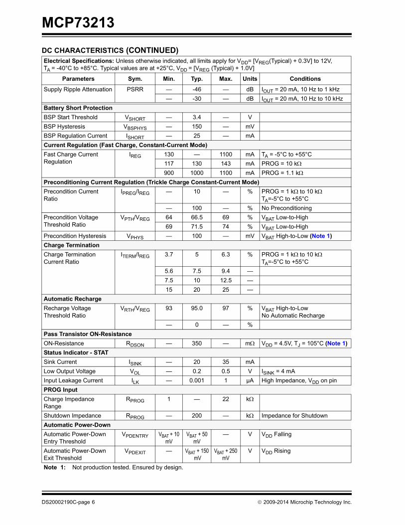
MCP73213
DS20002190C-page 6 2009-2014 Microchip Technology Inc.
Supply Ripple Attenuation PSRR — -46 — dB IOUT = 20 mA, 10 Hz to 1 kHz
— -30 — dB IOUT = 20 mA, 10 Hz to 10 kHz
Battery Short Protection
BSP Start Threshold VSHORT — 3.4 — V
BSP Hysteresis VBSPHYS — 150 — mV
BSP Regulation Current ISHORT — 25 — mA
Current Regulation (Fast Charge, Constant-Current Mode)
Fast Charge Current Regulation
IREG 130 — 1100 mA TA = -5°C to +55°C
117 130 143 mA PROG = 10 k
900 1000 1100 mA PROG = 1.1 k
Preconditioning Current Regulation (Trickle Charge Constant-Current Mode)
Precondition Current Ratio
IPREG/IREG — 10 — % PROG = 1 kto 10 kTA=-5°C to +55°C
— 100 — % No Preconditioning
Precondition Voltage Threshold Ratio
VPTH/VREG 64 66.5 69 % VBAT Low-to-High
69 71.5 74 % VBAT Low-to-High
Precondition Hysteresis VPHYS — 100 — mV VBAT High-to-Low (Note 1)
Charge Termination
Charge TerminationCurrent Ratio
ITERM/IREG 3.7 5 6.3 % PROG = 1 kto 10 kTA=-5°C to +55°C
5.6 7.5 9.4 —
7.5 10 12.5 —
15 20 25 —
Automatic Recharge
Recharge Voltage Threshold Ratio
VRTH/VREG 93 95.0 97 % VBAT High-to-LowNo Automatic Recharge
— 0 — %
Pass Transistor ON-Resistance
ON-Resistance RDSON — 350 — m VDD = 4.5V, TJ = 105°C (Note 1)
Status Indicator - STAT
Sink Current ISINK — 20 35 mA
Low Output Voltage VOL — 0.2 0.5 V ISINK = 4 mA
Input Leakage Current ILK — 0.001 1 µA High Impedance, VDD on pin
PROG Input
Charge Impedance Range
RPROG 1 — 22 k
Shutdown Impedance RPROG — 200 — k Impedance for Shutdown
Automatic Power-Down
Automatic Power-Down Entry Threshold
VPDENTRY VBAT + 10mV
VBAT + 50mV
— V VDD Falling
Automatic Power-Down Exit Threshold
VPDEXIT — VBAT + 150mV
VBAT + 250mV
V VDD Rising
DC CHARACTERISTICS (CONTINUED)Electrical Specifications: Unless otherwise indicated, all limits apply for VDD= [VREG(Typical) + 0.3V] to 12V, TA = -40°C to +85°C. Typical values are at +25°C, VDD = [VREG (Typical) + 1.0V]
Parameters Sym. Min. Typ. Max. Units Conditions
Note 1: Not production tested. Ensured by design.
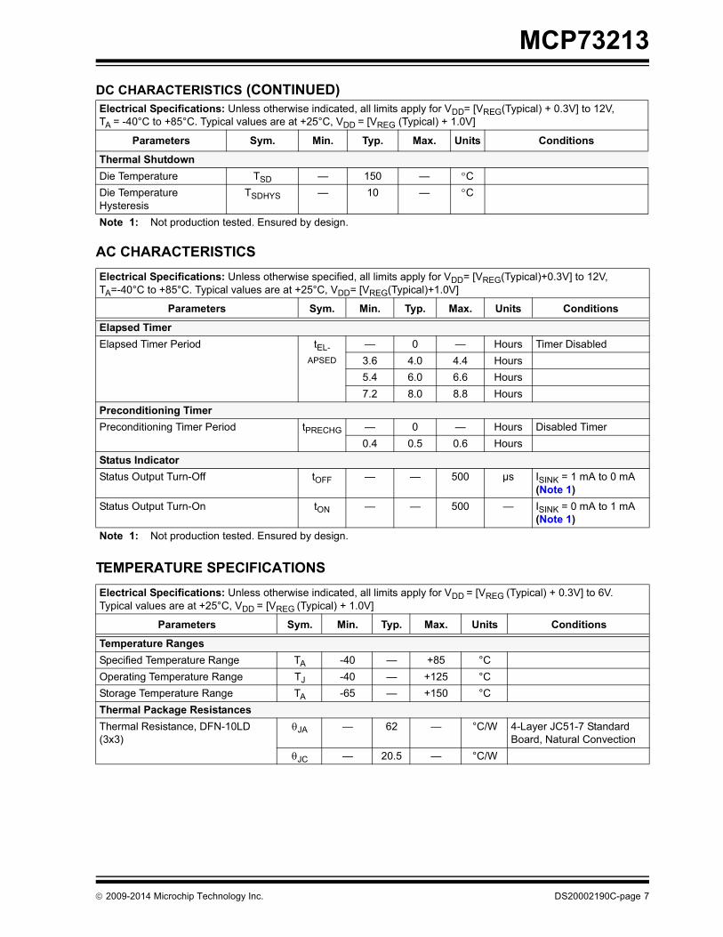
2009-2014 Microchip Technology Inc. DS20002190C-page 7
MCP73213
AC CHARACTERISTICS
TEMPERATURE SPECIFICATIONS
Thermal Shutdown
Die Temperature TSD — 150 — C
Die Temperature Hysteresis
TSDHYS — 10 — C
Electrical Specifications: Unless otherwise specified, all limits apply for VDD= [VREG(Typical)+0.3V] to 12V, TA=-40°C to +85°C. Typical values are at +25°C, VDD= [VREG(Typical)+1.0V]
Parameters Sym. Min. Typ. Max. Units Conditions
Elapsed Timer
Elapsed Timer Period tEL-
APSED
— 0 — Hours Timer Disabled
3.6 4.0 4.4 Hours
5.4 6.0 6.6 Hours
7.2 8.0 8.8 Hours
Preconditioning Timer
Preconditioning Timer Period tPRECHG — 0 — Hours Disabled Timer
0.4 0.5 0.6 Hours
Status Indicator
Status Output Turn-Off tOFF — — 500 µs ISINK = 1 mA to 0 mA (Note 1)
Status Output Turn-On tON — — 500 — ISINK = 0 mA to 1 mA (Note 1)
Note 1: Not production tested. Ensured by design.
Electrical Specifications: Unless otherwise indicated, all limits apply for VDD = [VREG (Typical) + 0.3V] to 6V.Typical values are at +25°C, VDD = [VREG (Typical) + 1.0V]
Parameters Sym. Min. Typ. Max. Units Conditions
Temperature Ranges
Specified Temperature Range TA -40 — +85 °C
Operating Temperature Range TJ -40 — +125 °C
Storage Temperature Range TA -65 — +150 °C
Thermal Package Resistances
Thermal Resistance, DFN-10LD (3x3)
JA — 62 — °C/W 4-Layer JC51-7 Standard Board, Natural Convection
JC — 20.5 — °C/W
DC CHARACTERISTICS (CONTINUED)Electrical Specifications: Unless otherwise indicated, all limits apply for VDD= [VREG(Typical) + 0.3V] to 12V, TA = -40°C to +85°C. Typical values are at +25°C, VDD = [VREG (Typical) + 1.0V]
Parameters Sym. Min. Typ. Max. Units Conditions
Note 1: Not production tested. Ensured by design.

MCP73213
DS20002190C-page 8 2009-2014 Microchip Technology Inc.
NOTES:

2009-2014 Microchip Technology Inc. DS20002190C-page 9
MCP73213
2.0 TYPICAL PERFORMANCE CURVES
Note: Unless otherwise indicated, VDD = [VREG(Typical) + 1V], IOUT = 50 mA and TA= +25°C, Constant Voltage mode.
FIGURE 2-1: Battery Regulation Voltage (VBAT) vs. Supply Voltage (VDD).
FIGURE 2-2: Battery Regulation Voltage (VBAT) vs. Supply Voltage (VDD).
FIGURE 2-3: Battery Regulation Voltage (VBAT) vs. Ambient Temperature (TA).
FIGURE 2-4: Battery Regulation Voltage (VBAT) vs. Ambient Temperature (TA).
FIGURE 2-5: Charge Current (IOUT) vs. Programming Resistor (RPROG).
FIGURE 2-6: Charge Current (IOUT) vs. Supply Voltage (VDD).
Note: The graphs and tables provided following this note are a statistical summary based on a limited number ofsamples and are provided for informational purposes only. The performance characteristics listed hereinare not tested or guaranteed. In some graphs or tables, the data presented may be outside the specifiedoperating range (e.g., outside specified power supply range) and therefore outside the warranted range.
8.16
8.17
8.18
8.19
8.20
8.21
8.22
8.23
8.24
8.4 9.0 9.6 10.2 10.8 11.4 12.0
Supply Voltage (V)
Ba
tte
ry R
egu
lati
on
Vo
lta
ge
(V
)
VBAT = 8.2VILOAD = 150 mATA = +25°C
8.16
8.17
8.18
8.19
8.20
8.21
8.22
8.23
8.24
8.4 9.0 9.6 10.2 10.8 11.4 12.0
Supply Voltage (V)
Ba
tte
ry R
egu
lati
on
Vo
lta
ge
(V
)
VBAT = 8.2VILOAD = 50 mATA = +25°C
8.16
8.17
8.18
8.19
8.20
8.21
8.22
8.23
8.24
-5 5 15 25 35 45 55
Ambient Temperature (°C)
Bat
tery
Reg
ula
tio
n V
olt
age
(V)
VBAT = 8.2VVDD = 9.2VILOAD = 50 mA
8.16
8.17
8.18
8.19
8.20
8.21
8.22
8.23
8.24
-5.0 5.0 15.0 25.0 35.0 45.0 55.0
Ambient Temperature (°C)
Bat
tery
Reg
ula
tio
n V
olt
age
(V)
VBAT = 8.2VVDD = 9.2VILOAD = 150 mA
0
200
400
600
800
1000
1200
1 3 5 7 9 11 13 15 17 19
Programming Resistor (kΩ)
Ch
arg
e C
urr
en
t (m
A)
VBAT = 8.2VVDD = 9.2VTA = +25°C
700720740760780800820840860880900
8.4 9.0 9.6 10.2 10.8 11.4 12.0
Supply Voltage (V)
Ch
arg
e C
urr
en
t (m
A)
RPROG = 1.3 kΩTA = +25°C

MCP73213
DS20002190C-page 10 2009-2014 Microchip Technology Inc.
TYPICAL PERFORMANCE CURVES (CONTINUED)Note: Unless otherwise indicated, VDD = [VREG(Typical) + 1V], IOUT = 10 mA and TA= +25°C, Constant-voltage mode.
FIGURE 2-7: Charge Current (IOUT) vs. Supply Voltage (VDD).
FIGURE 2-8: Charge Current (IOUT) vs. Supply Voltage (VDD).
FIGURE 2-9: Charge Current (IOUT) vs. Ambient Temperature (TA).
FIGURE 2-10: Charge Current (IOUT) vs. Ambient Temperature (TA).
FIGURE 2-11: Battery Short Protection Regulation Current (ISHORT) vs. Ambient Temperature (TA).
FIGURE 2-12: Output Leakage Current (IDISCHARGE) vs. Ambient Temperature (TA).
100106112118124130136142148154160
8.4 9.0 9.6 10.2 10.8 11.4 12.0
Supply Voltage (V)
Ch
arg
e C
urr
en
t (m
A)
RPROG = 10 kΩTA = +25°C
200210220230240250260270280290300
8.4 9.0 9.6 10.2 10.8 11.4 12.0
Supply Voltage (V)
Ch
arg
e C
urr
en
t (m
A)
RPROG = 5 kΩTA = +25°C
6063666972757881848790
-5 0 5 10 15 20 25 30 35 40 45 50 55
Ambient Temperature (°C)
Ch
arg
e C
urr
ent
(mA
)
VBAT = 8.2VRPROG = 20 kΩ
VDD = 12V
VDD = 11V
VDD = 8.5V
VDD = 9.2V
550
560
570
580
590
600
-5 0 5 10 15 20 25 30 35 40 45 50 55
Ambient Temperature (°C)
Ch
arg
e C
urr
ent
(mA
)
VDD = 8.5V
VDD = 9.2V
VDD = 11V
VDD = 12V
VBAT = 8.2VRPROG = 2 kΩ
10
14
18
22
26
30
-45 -35 -25 -15 -5 5 15 25 35 45 55 65 75 85
Ambient Temperature (C)
BS
P R
egu
lati
on
Cu
rre
nt
(mA
)
VDD = 9.2V
-1.00.01.02.03.04.05.06.07.08.09.0
-5.0 5.0 15.0 25.0 35.0 45.0 55.0
Ambient Temperature (°C)
Dis
char
ge
Cu
rren
t (u
A)
VDD < VBAT
VDD < VSTOP
End of Charge

2009-2014 Microchip Technology Inc. DS20002190C-page 11
MCP73213
TYPICAL PERFORMANCE CURVES (CONTINUED)Note: Unless otherwise indicated, VDD = [VREG(Typical) + 1V], IOUT = 10 mA and TA= +25°C, Constant-voltage mode.
FIGURE 2-13: Battery Voltage Accuracy (VRTOL) vs. Supply Voltage (VDD).
FIGURE 2-14: Load Transient Response (ILOAD = 50 mA/Div, Output: 100 mV/Div, Time: 100 µs/Div).
FIGURE 2-15: Complete Charge Cycle.
FIGURE 2-16: Input Overvoltage Protection.
FIGURE 2-17: Line Transient Response (ILOAD = 10 mA) (100 µs/Div).
FIGURE 2-18: Line Transient Response (ILOAD = 100 mA) (100 µs/Div).
-0.5
-0.3
-0.1
0.1
0.3
0.5
8.4 9.0 9.6 10.2 10.8 11.4 12.0
Supply Voltage (V)
Ba
tte
ry V
olt
ag
e A
cc
ura
cy
(%
)
VBAT = 8.2VILOAD = 150 mATA = +25°C
Output Ripple (V)
Output Current (mA)
0
1
2
3
4
5
6
7
8
9
10
0 10 20 30 40 50 60 70 80 90Time (Minutes)
Ba
tter
y V
olt
ag
e (
V)
00.10.20.30.40.50.60.70.80.911.11.2
Su
pp
ly C
urr
ent
(A)
VDD = 9VRPROG = 1.5 kΩ875 mAh Li-Ion Battery
Thermal Foldback
Input Voltage
Battery VoltageOutput Current
Output Ripple (V)
Source Voltage (V)
Output Ripple (V)
Source Voltage (V)

MCP73213
DS20002190C-page 12 2009-2014 Microchip Technology Inc.
NOTES:

2009-2014 Microchip Technology Inc. DS20002190C-page 13
MCP73213
3.0 PIN DESCRIPTIONThe descriptions of the pins are listed in Table 3-1.
TABLE 3-1: PIN FUNCTION TABLE
3.1 Battery Management Input Supply (VDD)
A supply voltage of [VREG (Typical) + 0.3V] to 13.0V isrecommended. Bypass to VSS with a minimum of 1 µF.The VDD pin is rated 18V absolute maximum to preventa sudden rise in input voltage from spikes or low-costAC-DC wall adapters from causing an over-voltagecondition and damaging the device.
3.2 Battery Charge Control Output (VBAT)
Connect to the positive terminal of the battery. Bypassto VSS with a minimum of 1 µF to ensure loop stabilitywhen the battery is disconnected.
3.3 No Connection (NC)
No connection.
3.4 Status Output (STAT)
STAT is an open-drain logic output for connection to anLED for charge status indication in stand-aloneapplications. Alternatively, a pull-up resistor can beapplied for interfacing to a host microcontroller. Refer toTable 5-2 for a summary of the status output during acharge cycle.
3.5 Battery Management 0V Reference (VSS)
Connect to the negative terminal of the battery andinput supply.
3.6 Current Regulation Set (PROG)
The fast charge current is set by placing a resistor fromPROG to VSS during constant current (CC) mode.PROG pin also serves as charge control enable. Whena typical 200 k impedance is applied to the PROGpin, the MCP73213 will go into standby mode until thehigh impedance is removed. Refer to Section 5.5“Constant-Current Mode - Fast Charge” for details.
3.7 Exposed Pad (EP)
Connect the Exposed Thermal Pad (EP) to theexposed copper area on the Printed Circuit Board(PCB) for thermal enhancement. Additional vias in thecopper area under the MCP73213 device can improveheat dissipation performance and simplify theassembly process.
MCP73213Symbol I/O Description
DFN-10
1, 2 VDD I Battery Management Input Supply Pin
3, 4 VBAT I/O Battery Charge Control Output Pin
5, 6 NC — No Connection Pin
7 STAT O Battery Charge Status Output Pin
8, 9 VSS — Battery Management 0V Reference Pin
10 PROG I/O Battery Charge Current Regulation Program and Charge Control Enable Pin
11 EP — Exposed Pad Pin

MCP73213
DS20002190C-page 14 2009-2014 Microchip Technology Inc.
NOTES:

2009-2014 Microchip Technology Inc. DS20002190C-page 15
MCP73213
4.0 DEVICE OVERVIEW
The MCP73213 are simple, but fully integrated linear charge management controllers. Figure 4-1 depicts theoperational flow algorithm.
FIGURE 4-1: The MCP73213 Flow Chart.
VBAT < VPTH
Timer Expired
SHUTDOWN MODEVDD < VUVLOVDD < VPD
orPROG > 200 kSTAT = High Z
TEMPERATURE FAULTNo Charge Current
STAT = Flashing (Type 2)STAT = High Z (Type 1)
Timer Suspended
TIMER FAULTNo Charge Current
STAT = Flashing (Type 2)STAT = High Z (Type 1)
Timer Suspended
PRECONDITIONING MODECharge Current = IPREG
STAT = LOWTimer ResetTimer Enable
FAST CHARGE MODECharge Current = IREG
STAT = LOW Timer Reset
Timer Enabled
CONSTANT VOLTAGE MODECharge Voltage = VREG
STAT = LOW
CHARGE COMPLETE MODENo Charge Current
STAT = High ZTimer Reset
VBAT > VPTH
VBAT = VREG
VBAT < ITERM
VBAT > VPTH
VBAT < VRTH
VDD < VOVP
VDD > VOVP
OVERVOLTAGE PROTECTIONNo Charge Current
STAT = High ZTimer Suspended
VDD > VOVP
VDD < VOVPVDD > VOVP
VDD < VOVP
Timer Expired
TIMER FAULTNo Charge Current
STAT = Flashing (Type 2)STAT = High Z (Type 1)
Timer Suspended
Die Temperature > TSD
Die Temperature < TSDHYS
Charge Mode Resume
BATTERY SHORT PROTECTIONCharge Current = ISHORTSTAT = Flashing (Type 2)STAT = High Z (Type 1)
Timer Suspended
VBAT > VSHORT
VBAT < VSHORT
Charge Mode Resume

MCP73213
DS20002190C-page 16 2009-2014 Microchip Technology Inc.
NOTES:

2009-2014 Microchip Technology Inc. DS20002190C-page 17
MCP73213
5.0 DETAILED DESCRIPTION
5.1 Undervoltage Lockout (UVLO)
An internal undervoltage lockout (UVLO) circuitmonitors the input voltage and keeps the charger inshutdown mode until the input supply rises above theUVLO threshold. In the event a battery is present whenthe input power is applied, the input supply must riseapproximately 150 mV above the battery voltagebefore the MCP73213 device becomes operational.
The UVLO circuit places the device in shutdown modeif the input supply falls to approximately 150 mV abovethe battery voltage.The UVLO circuit is always active.Any time the input supply is below the UVLO thresholdor approximately 150 mV of the voltage at the VBAT pin,the MCP73213 device is placed in a shutdown mode.
5.2 Overvoltage Protection (OVP)
An internal overvoltage protection (OVP) circuitmonitors the input voltage and keeps the charger inshutdown mode when the input supply rises above thetypical 13V OVP threshold. The OVP hysteresis isapproximately 150 mV for the MCP73213 device.
The MCP73213 device is operational between UVLOand OVP thresholds. The OVP circuit is also recog-nized as overvoltage lockout (OVLO).
5.3 Charge Qualification
When the input power is applied, the input supply mustrise 150 mV above the battery voltage before theMCP73213 becomes operational.
The automatic power-down circuit places the device ina shutdown mode if the input supply falls to within+50 mV of the battery voltage.
The automatic circuit is always active. At any time theinput supply is within +50 mV of the voltage at the VBATpin, the MCP73213 is placed in a shutdown mode.
For a charge cycle to begin, the automaticpower-down conditions must be met and the chargeenable input must be above the input high threshold.
5.3.1 BATTERY MANAGEMENT INPUT SUPPLY (VDD)
The VDD input is the input supply to the MCP73213. TheMCP73213 automatically enters a power-down mode ifthe voltage on the VDD input falls to within +50 mV of thebattery voltage. This feature prevents draining thebattery pack when the VDD supply is not present.
5.3.2 BATTERY CHARGE CONTROL OUTPUT (VBAT)
The battery charge control output is the drain terminalof an internal P-channel MOSFET. The MCP73213provides constant current and voltage regulation to thebattery pack by controlling this MOSFET in the linearregion. The battery charge control output should beconnected to the positive terminal of the battery pack.
5.3.3 BATTERY DETECTION
The MCP73213 detects the battery presence withcharging of the output capacitor. The charge flow willinitiate when the voltage on VBAT is pulled below theVRECHARGE threshold. Refer to Section 1.0 “ElectricalCharacteristics” for VRECHARGE values. The value willbe the same for nonrechargeable devices.
When VBAT > VREG + Hysteresis, the charge will besuspended (or not started, depending on the condition)to prevent overcharging.
5.4 Preconditioning
If the voltage at the VBAT pin is less than thepreconditioning threshold, the MCP73213 deviceenters a preconditioning mode. The preconditioningthreshold is factory set. Refer to Section 1.0“Electrical Characteristics” for preconditioningthreshold options.
In this mode, the MCP73213 device supplies 10% ofthe fast charge current (established with the value ofthe resistor connected to the PROG pin) to the battery.
When the voltage at the VBAT pin rises above thepreconditioning threshold, the MCP73213 deviceenters the Constant Current (Fast Charge) mode.
5.4.1 TIMER EXPIRED DURING PRECONDITIONING MODE
If the internal timer expires before the voltage thresholdis reached for Fast Charge mode, a timer fault isindicated and the charge cycle terminates. TheMCP73213 device remains in this condition until the bat-tery is removed or input power is cycled. If the battery isremoved, the MCP73213 device enters the Standbymode, where it remains until a battery is reinserted.
Note: The MCP73213 device also offers optionswith no preconditioning.
Note: The typical preconditioning timer forMCP73213 is 32 minutes. TheMCP73213 also offers options with nopreconditioning timer.

MCP73213
DS20002190C-page 18 2009-2014 Microchip Technology Inc.
5.5 Constant-Current Mode - Fast Charge
During Constant-Current mode, the programmedcharge current is supplied to the battery or load.
The charge current is established using a singleresistor from PROG to VSS. The program resistor andthe charge current are calculated using the followingequation:
EQUATION 5-1:
EQUATION 5-2:
Table 5-1 provides commonly seen E96 (1%) and E24(5%) resistors for various charge current to reducedesign time.
Constant-Current mode is maintained until the voltageat the VBAT pin reaches the regulation voltage, VREG.When Constant Current mode is invoked, the internaltimer is reset.
5.5.1 TIMER EXPIRED DURING CONSTANT-CURRENT - FAST CHARGE MODE
If the internal timer expires before the recharge voltagethreshold is reached, a timer fault is indicated and thecharge cycle terminates. The MCP73213 deviceremains in this condition until the battery is removed. Ifthe battery is removed or input power is cycled, theMCP73213 device enters the Standby mode where itremains until a battery is reinserted.
5.6 Constant-Voltage Mode
When the voltage at the VBAT pin reaches theregulation voltage, VREG, constant voltage regulationbegins. The regulation voltage is factory set to 8.2V,8.4V, 8.7V or 8.8V with a tolerance of ± 0.5%.
5.7 Charge Termination
The charge cycle is terminated when, during Constant-Voltage mode, the average charge current diminishesbelow a threshold established with the value of 5%,7.5%, 10% or 20% of fast charge current or the internaltimer expires. A 1 ms filter time on the termination com-parator ensures that transient load conditions do notresult in premature charge cycle termination. The timerperiod is factory set and can be disabled. Refer toSection 1.0 “Electrical Characteristics” for timerperiod options.
5.8 Automatic Recharge
The MCP73213 device continuously monitors thevoltage at the VBAT pin in the charge complete mode. Ifthe voltage drops below the recharge threshold,another charge cycle begins and current is once againsupplied to the battery or load. The recharge thresholdis factory set. Refer to Section 1.0 “ElectricalCharacteristics” for recharge threshold options.
For the MCP73213 device with no recharge option, theMCP73213 will go into Standby mode when the termi-nation condition is met. The charge will not restart untilthe following conditions have been met:
• Battery is removed from the system and inserted again
• VDD is removed and plugged in again
• RPROG is disconnected (or high-impedance) and reconnected
TABLE 5-1: RESISTOR LOOKUP TABLE
Charge Current (mA)
Recommended E96 Resistor ()
Recommended E24 Resistor ()
130 10k 10k
150 8.45k 8.20k
200 6.20k 6.20k
250 4.99k 5.10k
300 4.02k 3.90k
350 3.40k 3.30k
400 3.00k 3.00k
450 2.61k 2.70k
500 2.32k 2.37k
550 2.10k 2.20k
600 1.91k 2.00k
650 1.78k 1.80k
700 1.62k 1.60k
750 1.50k 1.50k
800 1.40k 1.50k
850 1.33k 1.30k
900 1.24k 1.20k
950 1.18k 1.20k
1000 1.10k 1.10k
1100 1.00k 1.00k
IREG 1104 RPROG0.93–=
Where:
RPROG = kilohm (k)
IREG = milliampere (mA)
RPROG 10
IREG
1104------------ log
0.93– =
Where:
RPROG = kilohm (k)
IREG = milliampere (mA)
Note: The MCP73213 also offers options withno automatic recharge.

2009-2014 Microchip Technology Inc. DS20002190C-page 19
MCP73213
5.9 Thermal Regulation
The MCP73213 shall limit the charge current based onthe die temperature. The thermal regulation optimizesthe charge cycle time while maintaining devicereliability. Figure 5-1 depicts the thermal regulation forthe MCP73213 device. Refer to Section 1.0“Electrical Characteristics” for thermal packageresistances and Section 6.1.1.2 “ThermalConsiderations” for calculating power dissipation..
FIGURE 5-1: Thermal Regulation.
5.10 Thermal Shutdown
The MCP73213 suspends charge if the dietemperature exceeds +150°C. Charging will resumewhen the die temperature has cooled by approximately10°C. The thermal shutdown is a secondary safetyfeature in the event that there is a failure within thethermal regulation circuitry.
5.11 Status Indicator
The charge status outputs are open-drain outputs withtwo different states: Low (L), and High-Impedance(High Z). The charge status outputs can be used toilluminate LEDs. Optionally, the charge status outputscan be used as an interface to a host microcontroller.Table 5-2 summarizes the state of the status outputsduring a charge cycle.
5.12 Battery Short Protection
Once a single-cell Li-Ion battery is detected, an internalbattery short protection (BSP) circuit starts monitoringthe battery voltage. When VBAT falls below a typical1.7V battery short protection threshold voltage, thecharging behavior is postponed. A typical 25 mAdetection current is supplied for recovering from thebattery short condition.
Preconditioning mode resumes when VBAT raisesabove the battery short protection threshold. The bat-tery voltage must rise approximately 150 mV above thebattery short protection voltage before the MCP73213device becomes operational.
0
30
60
90
120
150
25 40 55 70 85 100 115 130 145 160Junction Temperature (°C)
Fa
st C
har
ge
Cu
rren
t (m
A)
VDD = 9.1VRPROG = 10 kΩ
TABLE 5-2: STATUS OUTPUTS
CHARGE CYCLE STATE
STAT
Shutdown High Z
Standby High Z
Preconditioning L
Constant Current Fast Charge
L
Constant Voltage L
Charge Complete - Standby High Z
Temperature Fault 1.6 second 50% D.C.Flashing (Type 2)High Z (Type 1)
Timer Fault 1.6 second 50% D.C.Flashing (Type 2)High Z (Type 1)
Preconditioning Timer Fault 1.6 second 50% D.C.Flashing (Type 2)High Z (Type 1)

MCP73213
DS20002190C-page 20 2009-2014 Microchip Technology Inc.
NOTES:

2009-2014 Microchip Technology Inc. DS20002190C-page 21
MCP73213
6.0 APPLICATIONS
The MCP73213 is designed to operate in conjunctionwith a host microcontroller or in stand-aloneapplications. The MCP73213 provides the preferredcharge algorithm for dual Lithium-Ion orLithium-Polymer cells: Constant Current followed byConstant Voltage. Figure 6-1 depicts a typicalstand-alone application circuit, while Figure 6-2depicts the accompanying charge profile.
FIGURE 6-1: Typical Application Circuit.
FIGURE 6-2: Typical Charge Profile (875 mAh Li-Ion Battery).
VDD
5
31
2
8
7
RPROG9
10
CINCOUT
RLED
+
-
2-Cell Li-Ion Battery
6
4
MC
P7
321
3
VDD
STAT
NC
NC
VBAT
VBAT
PROG
VSS
VSS
AC-DC-Adapter
0
1
2
3
4
5
6
7
8
9
10
0 10 20 30 40 50 60 70 80 90Time (Minutes)
Ba
tte
ry V
olt
ag
e (
V)
00.10.20.30.40.50.60.70.80.911.11.2
Su
pp
ly C
urr
en
t (A
)
VDD = 9VRPROG = 1.5 kΩ875 mAh Li-Ion Battery
Thermal Foldback

MCP73213
DS20002190C-page 22 2009-2014 Microchip Technology Inc.
6.1 Application Circuit Design
Due to the low efficiency of linear charging, the mostimportant factors are thermal design and cost, whichare a direct function of the input voltage, output currentand thermal impedance between the battery chargerand the ambient cooling air. The worst-case situation iswhen the device has transitioned from thePreconditioning mode to the Constant Current mode. Inthis situation, the battery charger has to dissipate themaximum power. A trade-off must be made betweenthe charge current, cost and thermal requirements ofthe charger.
6.1.1 COMPONENT SELECTION
Selection of the external components in Figure 6-1 iscrucial to the integrity and reliability of the chargingsystem. The following discussion is intended as a guidefor the component selection process.
6.1.1.1 Charge Current
The preferred fast charge current for Li-Ion/Li-Poly cellsis below the 1C rate, with an absolute maximum currentat the 2C rate. The recommended fast charge cur-rent should be obtained from the batterymanufacturer. For example, a 500 mAh battery packwith 0.7C preferred fast charge current has a chargecurrent of 350 mA. Charging at this rate provides theshortest charge cycle times without degradation to thebattery pack performance or life.
6.1.1.2 Thermal Considerations
The worst-case power dissipation in the batterycharger occurs when the input voltage is at themaximum and the device has transitioned fromPreconditioning mode to Constant-Current mode. Inthis case, the power dissipation is:
EQUATION 6-1:
Power dissipation with a 9V, ±10% input voltagesource, 400 mA ±10% and preconditioning thresholdvoltage at 6V is:
EQUATION 6-2:
This power dissipation with the battery charger in theDFN-10 package will result approximately 98C aboveroom temperature.
6.1.1.3 External Capacitors
The MCP73213 is stable with or without a battery load.In order to maintain good AC stability in Constant-Volt-age mode, a minimum capacitance of 1 µF isrecommended to bypass the VBAT pin to VSS. Thiscapacitance provides compensation when there is nobattery load. In addition, the battery andinterconnections appear inductive at high frequencies.These elements are in the control feedback loop duringConstant Voltage mode. Therefore, bypasscapacitance may be necessary to compensate for theinductive nature of the battery pack.
For typical applications, it is recommended to apply aminimum of 16V rated 1 µF to the output capacitor anda minimum of 25V rated 1 µF to the input capacitor.
TABLE 6-1: MLCC CAPACITOR EXAMPLE
Virtually any good quality output filter capacitor can beused independent of the capacitor’s minimum EffectiveSeries Resistance (ESR) value. The actual value of thecapacitor (and its associated ESR) depends on the out-put load current. A 1 µF ceramic, tantalum or aluminumelectrolytic capacitor at the output is usually sufficientto ensure stability.
6.1.1.4 Reverse-Blocking Protection
The MCP73213 provides protection from a faulted orshorted input. Without the protection, a faulted orshorted input would discharge the battery pack throughthe body diode of the internal pass transistor.
Note: Please consult with your battery supplieror refer to the battery data sheet for thepreferred charge rate.
PowerDissipation VDDMAX VPTHMIN– IREGMAX=
Where:
VDDMAX = the maximum input voltage
IREGMAX = the maximum fast charge current
VPTHMIN = the minimum transition threshold voltage
MLCC Capacitors
Temperature Range
Tolerance
X7R -55C to +125C ±15%
X5R -55C to +85C ±15%
Power dissipation 9.9V 6.0V– 440 mA 1.58W==

2009-2014 Microchip Technology Inc. DS20002190C-page 23
MCP73213
6.2 PCB Layout Issues
For optimum voltage regulation, place the battery packas close as possible to the device’s VBAT and VSS pinsto minimize voltage drops along the high-current-carrying PCB traces.
If the PCB layout is used as a heatsink, adding multiplevias in the heatsink pad can help conduct more heat tothe backplane of the PCB, thus reducing the junctiontemperature. Figures 6-4 and 6-5 depict a typical layoutwith PCB heatsinking.
FIGURE 6-3: Typical Layout (Top).
FIGURE 6-4: Typical Layout (Top Metal).
FIGURE 6-5: Typical Layout (Bottom).
102-00261MCP73213EV

MCP73213
DS20002190C-page 24 2009-2014 Microchip Technology Inc.
NOTES:

2009-2014 Microchip Technology Inc. DS20002190C-page 25
MCP73213
7.0 PACKAGING INFORMATION
7.1 Package Marking Information
XXXX
10-Lead DFN (3x3)
YYWW
NNN
Example:
Standard *
Part Number Code
MCP73213-A6SI/MF Z3HI
MCP73213T-A6SI/MF Z3HI
MCP73213-B6SI/MF Y3HI
MCP73213T-B6SI/MF Y3HI
Z3HI
1443
256
Legend: XX...X Customer-specific informationY Year code (last digit of calendar year)YY Year code (last 2 digits of calendar year)WW Week code (week of January 1 is week ‘01’)NNN Alphanumeric traceability code Pb-free JEDEC® designator for Matte Tin (Sn)* This package is Pb-free. The Pb-free JEDEC designator ( )
can be found on the outer packaging for this package.
Note: In the event the full Microchip part number cannot be marked on one line, it willbe carried over to the next line, thus limiting the number of availablecharacters for customer-specific information.
3e
3e

MCP73213
DS20002190C-page 26 2009-2014 Microchip Technology Inc.
Note: For the most current package drawings, please see the Microchip Packaging Specification located at http://www.microchip.com/packaging

2009-2014 Microchip Technology Inc. DS20002190C-page 27
MCP73213
Note: For the most current package drawings, please see the Microchip Packaging Specification located at http://www.microchip.com/packaging

MCP73213
DS20002190C-page 28 2009-2014 Microchip Technology Inc.
Note: For the most current package drawings, please see the Microchip Packaging Specification located at http://www.microchip.com/packaging
2009-2014 Microchip Technology Inc. DS20002190C-page 29
MCP73213
APPENDIX A: REVISION HISTORY
Revision C (December 2014)
The following is the list of modifications:
1. Added Note 7 in Table 1 regarding the Type 1and Type 2 descriptions.
2. Updated the Functional Block Diagram.
3. Updated the thermal resistances in the Temperature Specifications.
4. Changed captions for the Figures 2-7, 2-8, 2-15,2-16.
5. Updated Figure 4-1.
6. Updated Section 6.1.1.2, Thermal Considerations.
7. Updated Section 7.1, Package MarkingInformation.
8. Minor typographical corrections.
Revision B (December 2009)
The following is the list of modifications:
1. Updated the Battery Short Protection values inthe DC Characteristics table.
Revision A (July 2009)
• Original Release of this Document.

MCP73213
DS20002190C-page 30 2009-2014 Microchip Technology Inc.
NOTES:

2009-2014 Microchip Technology Inc. DS20002190C-page 31
MCP73213
PRODUCT IDENTIFICATION SYSTEM
To order or obtain information, e.g., on pricing or delivery, refer to the factory or the listed sales office.
Device: MCP73213-xxx: Dual Cell Li-Ion/Li-Polymer Battery DeviceMCP73213T-xxx: Dual Cell Li-Ion/Li-Polymer Battery Device,
Tape and Reel
Tape and ReelOption:
T = Tape and Reel(1)
TemperatureRange:
I = -40C to +85C (Industrial)
Package: MF = 10-Lead Plastic Dual Flat, No Lead - 3x3 mm Body (DFN)
Examples:
a) MCP73213-A6SI/MF: Dual Cell Li-Ion/Li-Polymer Battery Device
b) MCP73213-B6SI/MF: Dual Cell Li-Ion/Li-Polymer Battery Device
c) MCP73213T-A6SI/MF: Tape and Reel,Dual Cell Li-Ion/Li-Polymer Battery Device
d) MCP73213T-B6SI/MF: Tape and Reel,Dual Cell Li-Ion/Li-Polymer Battery Device
PART NO. X /XX XXX
PatternPackageTemperatureRange
Device
[X](1)
Tape and ReelOption
Note 1: Tape and Reel identifier only appears in the catalog part number description. This identifier is used for ordering purposes and is not printed on the device package. Check with your Microchip Sales Office for package availability with the Tape and Reel option.

MCP73213
DS20002190C-page 32 2009-2014 Microchip Technology Inc.
NOTES:

2009-2014 Microchip Technology Inc. DS20002190C-page 33
Information contained in this publication regarding deviceapplications and the like is provided only for your convenienceand may be superseded by updates. It is your responsibility toensure that your application meets with your specifications.MICROCHIP MAKES NO REPRESENTATIONS ORWARRANTIES OF ANY KIND WHETHER EXPRESS ORIMPLIED, WRITTEN OR ORAL, STATUTORY OROTHERWISE, RELATED TO THE INFORMATION,INCLUDING BUT NOT LIMITED TO ITS CONDITION,QUALITY, PERFORMANCE, MERCHANTABILITY ORFITNESS FOR PURPOSE. Microchip disclaims all liabilityarising from this information and its use. Use of Microchipdevices in life support and/or safety applications is entirely atthe buyer’s risk, and the buyer agrees to defend, indemnify andhold harmless Microchip from any and all damages, claims,suits, or expenses resulting from such use. No licenses areconveyed, implicitly or otherwise, under any Microchipintellectual property rights.
Trademarks
The Microchip name and logo, the Microchip logo, dsPIC, FlashFlex, flexPWR, JukeBlox, KEELOQ, KEELOQ logo, Kleer, LANCheck, MediaLB, MOST, MOST logo, MPLAB, OptoLyzer, PIC, PICSTART, PIC32 logo, RightTouch, SpyNIC, SST, SST Logo, SuperFlash and UNI/O are registered trademarks of Microchip Technology Incorporated in the U.S.A. and other countries.
The Embedded Control Solutions Company and mTouch are registered trademarks of Microchip Technology Incorporated in the U.S.A.
Analog-for-the-Digital Age, BodyCom, chipKIT, chipKIT logo, CodeGuard, dsPICDEM, dsPICDEM.net, ECAN, In-Circuit Serial Programming, ICSP, Inter-Chip Connectivity, KleerNet, KleerNet logo, MiWi, MPASM, MPF, MPLAB Certified logo, MPLIB, MPLINK, MultiTRAK, NetDetach, Omniscient Code Generation, PICDEM, PICDEM.net, PICkit, PICtail, RightTouch logo, REAL ICE, SQI, Serial Quad I/O, Total Endurance, TSHARC, USBCheck, VariSense, ViewSpan, WiperLock, Wireless DNA, and ZENA are trademarks of Microchip Technology Incorporated in the U.S.A. and other countries.
SQTP is a service mark of Microchip Technology Incorporated in the U.S.A.
Silicon Storage Technology is a registered trademark of Microchip Technology Inc. in other countries.
GestIC is a registered trademarks of Microchip Technology Germany II GmbH & Co. KG, a subsidiary of Microchip Technology Inc., in other countries.
All other trademarks mentioned herein are property of their respective companies.
© 2009-2014, Microchip Technology Incorporated, Printed in the U.S.A., All Rights Reserved.
ISBN: 978-1-63276-867-4
Note the following details of the code protection feature on Microchip devices:
• Microchip products meet the specification contained in their particular Microchip Data Sheet.
• Microchip believes that its family of products is one of the most secure families of its kind on the market today, when used in the intended manner and under normal conditions.
• There are dishonest and possibly illegal methods used to breach the code protection feature. All of these methods, to our knowledge, require using the Microchip products in a manner outside the operating specifications contained in Microchip’s Data Sheets. Most likely, the person doing so is engaged in theft of intellectual property.
• Microchip is willing to work with the customer who is concerned about the integrity of their code.
• Neither Microchip nor any other semiconductor manufacturer can guarantee the security of their code. Code protection does not mean that we are guaranteeing the product as “unbreakable.”
Code protection is constantly evolving. We at Microchip are committed to continuously improving the code protection features of ourproducts. Attempts to break Microchip’s code protection feature may be a violation of the Digital Millennium Copyright Act. If such actsallow unauthorized access to your software or other copyrighted work, you may have a right to sue for relief under that Act.
Microchip received ISO/TS-16949:2009 certification for its worldwide headquarters, design and wafer fabrication facilities in Chandler and Tempe, Arizona; Gresham, Oregon and design centers in California and India. The Company’s quality system processes and procedures are for its PIC® MCUs and dsPIC® DSCs, KEELOQ® code hopping devices, Serial EEPROMs, microperipherals, nonvolatile memory and analog products. In addition, Microchip’s quality system for the design and manufacture of development systems is ISO 9001:2000 certified.
QUALITY MANAGEMENT SYSTEM CERTIFIED BY DNV
== ISO/TS 16949 ==

DS20002190C-page 34 2009-2014 Microchip Technology Inc.
AMERICASCorporate Office2355 West Chandler Blvd.Chandler, AZ 85224-6199Tel: 480-792-7200 Fax: 480-792-7277Technical Support: http://www.microchip.com/supportWeb Address: www.microchip.com
AtlantaDuluth, GA Tel: 678-957-9614 Fax: 678-957-1455
Austin, TXTel: 512-257-3370
BostonWestborough, MA Tel: 774-760-0087 Fax: 774-760-0088
ChicagoItasca, IL Tel: 630-285-0071 Fax: 630-285-0075
ClevelandIndependence, OH Tel: 216-447-0464 Fax: 216-447-0643
DallasAddison, TX Tel: 972-818-7423 Fax: 972-818-2924
DetroitNovi, MI Tel: 248-848-4000
Houston, TX Tel: 281-894-5983
IndianapolisNoblesville, IN Tel: 317-773-8323Fax: 317-773-5453
Los AngelesMission Viejo, CA Tel: 949-462-9523 Fax: 949-462-9608
New York, NY Tel: 631-435-6000
San Jose, CA Tel: 408-735-9110
Canada - TorontoTel: 905-673-0699 Fax: 905-673-6509
ASIA/PACIFICAsia Pacific OfficeSuites 3707-14, 37th FloorTower 6, The GatewayHarbour City, KowloonHong KongTel: 852-2943-5100Fax: 852-2401-3431
Australia - SydneyTel: 61-2-9868-6733Fax: 61-2-9868-6755
China - BeijingTel: 86-10-8569-7000 Fax: 86-10-8528-2104
China - ChengduTel: 86-28-8665-5511Fax: 86-28-8665-7889
China - ChongqingTel: 86-23-8980-9588Fax: 86-23-8980-9500
China - HangzhouTel: 86-571-8792-8115 Fax: 86-571-8792-8116
China - Hong Kong SARTel: 852-2943-5100 Fax: 852-2401-3431
China - NanjingTel: 86-25-8473-2460Fax: 86-25-8473-2470
China - QingdaoTel: 86-532-8502-7355Fax: 86-532-8502-7205
China - ShanghaiTel: 86-21-5407-5533 Fax: 86-21-5407-5066
China - ShenyangTel: 86-24-2334-2829Fax: 86-24-2334-2393
China - ShenzhenTel: 86-755-8864-2200 Fax: 86-755-8203-1760
China - WuhanTel: 86-27-5980-5300Fax: 86-27-5980-5118
China - XianTel: 86-29-8833-7252Fax: 86-29-8833-7256
China - XiamenTel: 86-592-2388138 Fax: 86-592-2388130
China - ZhuhaiTel: 86-756-3210040 Fax: 86-756-3210049
ASIA/PACIFICIndia - BangaloreTel: 91-80-3090-4444 Fax: 91-80-3090-4123
India - New DelhiTel: 91-11-4160-8631Fax: 91-11-4160-8632
India - PuneTel: 91-20-3019-1500
Japan - OsakaTel: 81-6-6152-7160 Fax: 81-6-6152-9310
Japan - TokyoTel: 81-3-6880- 3770 Fax: 81-3-6880-3771
Korea - DaeguTel: 82-53-744-4301Fax: 82-53-744-4302
Korea - SeoulTel: 82-2-554-7200Fax: 82-2-558-5932 or 82-2-558-5934
Malaysia - Kuala LumpurTel: 60-3-6201-9857Fax: 60-3-6201-9859
Malaysia - PenangTel: 60-4-227-8870Fax: 60-4-227-4068
Philippines - ManilaTel: 63-2-634-9065Fax: 63-2-634-9069
SingaporeTel: 65-6334-8870Fax: 65-6334-8850
Taiwan - Hsin ChuTel: 886-3-5778-366Fax: 886-3-5770-955
Taiwan - KaohsiungTel: 886-7-213-7830
Taiwan - TaipeiTel: 886-2-2508-8600 Fax: 886-2-2508-0102
Thailand - BangkokTel: 66-2-694-1351Fax: 66-2-694-1350
EUROPEAustria - WelsTel: 43-7242-2244-39Fax: 43-7242-2244-393Denmark - CopenhagenTel: 45-4450-2828 Fax: 45-4485-2829
France - ParisTel: 33-1-69-53-63-20 Fax: 33-1-69-30-90-79
Germany - DusseldorfTel: 49-2129-3766400
Germany - MunichTel: 49-89-627-144-0 Fax: 49-89-627-144-44
Germany - PforzheimTel: 49-7231-424750
Italy - Milan Tel: 39-0331-742611 Fax: 39-0331-466781
Italy - VeniceTel: 39-049-7625286
Netherlands - DrunenTel: 31-416-690399 Fax: 31-416-690340
Poland - WarsawTel: 48-22-3325737
Spain - MadridTel: 34-91-708-08-90Fax: 34-91-708-08-91
Sweden - StockholmTel: 46-8-5090-4654
UK - WokinghamTel: 44-118-921-5800Fax: 44-118-921-5820
Worldwide Sales and Service
03/25/14

Mouser Electronics
Authorized Distributor
Click to View Pricing, Inventory, Delivery & Lifecycle Information: Microchip:
MCP73213-A6SI/MF MCP73213-B6SI/MF MCP73213T-A6SI/MF MCP73213T-B6SI/MF MCP73213-A6BI/MF
MCP73213T-B6AI/MF MCP73213-A6W/MF MCP73213-A6AI/MF MCP73213T-A6X/MF MCP73213T-A6AI/MF
MCP73213T-A6W/MF MCP73213T-G6AI/MF MCP73213T-G6XI/MF MCP73213-G6AI/MF MCP73213-A5JI/MF
MCP73213T-A6BI/MF MCP73213-A61I/MF MCP73213-A21I/MF MCP73213T-A61I/MF MCP73213-F6TI/MF
MCP73213T-A5JI/MF MCP73213T-F6TI/MF MCP73213T-A21I/MF MCP73213-B6AI/MF MCP73213-G6XI/MF
MCP73213-A6X/MF MCP73213TA6W MCP73213A6W