查询IMP16C552供应商 捷多邦,专业PCB打样工厂,24小时加急...
34
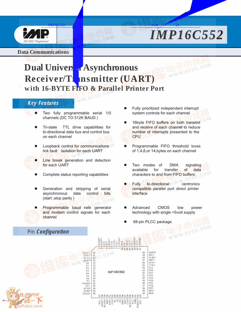
Two fully programmable serial 1/0 channels (DC TO 512K BAUD ) Tri-state TTL drive capabilities for bi-directional data bus and control bus on each channel Loopback control for communications link fault isolation for each UART Line break generation and detection for each UART Complete status reporting capabilities Generation and stripping of serial asynchronous data control bits (start ,stop parity ) Programmable baud rate generator and modem control signals for each channel Fully prioritized independent interrupt system controls for each channel 16byte FIFO buffers on both transmit and receive of each channel to reduce number of interrupts presented to the CPU Programmable FIFO threshold loves of 1,4,8,or 14,bytes on each channel Two modes of DMA signaling available for transfer of data characters to and from FIFO buffers Fully bi-directional centronics compatible parallel port direct printer interface Advanced CMOS low power technology with single +5voit supply 68-pin PLCC package Data Communications IMP16C552 IMP16C552 Key Features Dual Universal Asynchronous Receiver/Transmitter (UART) with 16-BYTE FIFO & Parallel Printer Port Pin Configuration . . 10 11 12 13 14 15 16 17 18 19 20 21 22 23 24 25 26 SOUT1 DTR1* RTS1* DSR1* D0 D1 D2 D3 D4 D5 D6 D7 TXRdy0* VCC RTS0* DTR0* SOUT0 DSR*D INT2 SLIN*+ INIT*+ AFD*+ STB*+ VSS PD0 PD1 PD2 PD3 PD4 PD5 PD6 PD7 INT0 BDO VSS DSRO* RLSD0* RI0* DSR* CSO* A2 A1 AO IOW* IOR* CSO* RESET• VCC SIN0 TXRDy1* VSS Rxrdy0* RISD1* VSS RI1* DSR1* CLK CSO) VSS LPTOE* ACK PE BUSY SLCT VCC ERROR* STS1 RXRdy1 27 28 29 30 31 32 33 34 35 36 37 38 39 40 41 42 43 9 8 7 6 5 4 3 2 1 68 67 66 65 64 63 62 61 16C552 60 59 58 57 56 55 54 53 52 51 50 49 48 47 46 45 44 IMP 查询IMP16C552供应商 捷多邦,专业PCB打样工厂,24小时加急出货
Transcript of 查询IMP16C552供应商 捷多邦,专业PCB打样工厂,24小时加急...
� Two fully programmable serial 1/0
channels (DC TO 512K BAUD ) � Tri-state TTL drive capabilities for
bi-directional data bus and control bus on each channel
� Loopback control for communications
link fault isolation for each UART � Line break generation and detection
for each UART � Complete status reporting capabilities � Generation and stripping of serial
asynchronous data control bits (start ,stop parity )
� Programmable baud rate generator
and modem control signals for each channel
� Fully prioritized independent interrupt system controls for each channel
� 16byte FIFO buffers on both transmit
and receive of each channel to reduce number of interrupts presented to the CPU
� Programmable FIFO threshold loves
of 1,4,8,or 14,bytes on each channel � Two modes of DMA signaling
available for transfer of data characters to and from FIFO buffers
� Fully bi-directional centronics
compatible parallel port direct printer interface
� Advanced CMOS low power
technology with single +5voit supply � 68-pin PLCC package
1 408-432-9100/www.impweb.com © 2002 IMP, Inc.
Data Communications
IMP16C552IMP16C552
Key Features
Dual Universal Asynchronous
Receiver/Transmitter (UART)
with 16-BYTE FIFO & Parallel Printer Port
Pin Configuration
.
.
1011121314151617181920212223242526
SOUT1DTR1*RTS1*DSR1*
D0D1D2D3D4D5D6D7
TXRdy0*VCC
RTS0*DTR0*
SOUT0
DSR*DINT2SLIN*+INIT*+AFD*+STB*+VSSPD0PD1PD2PD3PD4PD5PD6PD7INT0BDO
VS
SD
SR
O*
RLS
D0*
RI0
*D
SR
*C
SO
*A
2 A1
AO
IOW
*IO
R*
CS
O*
RE
SE
T•
VC
CS
IN0
TX
RD
y1*
VS
S
Rxr
dy0*
RIS
D1*
VS
SR
I1*
DS
R1*
CLK
CS
O)
VS
SLP
TO
E*
AC
KP
EB
US
YS
LCT
VC
CE
RR
OR
*S
TS
1R
XR
dy1
27 28 29 30 31 32 33 34 35 36 37 38 39 40 41 42 43
9 8 7 6 5 4 3 2 1 68 67 66 65 64 63 62 61
16C552
6059585756555453525150494847464544
IMP
查询IMP16C552供应商 捷多邦,专业PCB打样工厂,24小时加急出货
The low power COMS IMP16C522 is a single device solution for serving two serial input/output ports simultaneously and one fully bi-directional parallel port for the IBM PC ATM PS/2 and compatible systems. The parallel port is full compatible to the Centronics printer port and IBM serial parallel Adapter. Each Universal Asynchronous Receiver and transmitter (UART) is fully programmable. Each UART in the IMP16C522 is capable of buffering up to 16 bytes of data upon reception,relieving the CPU of interrupt overhead.Buffering of data also allows greater latencytime in interrupt servicing which is vitalin a multitasking environment, DMA signalingbetween the internal FIFO buffers and hostCPU allows single or multiple charactertransfers. Each UART has a maximumrecommended data rate of 256k with a clockfrequency of 80MHZ The IMP16C552 is an enhanced dual channel version of the IMP16C550A Universal
Asynchronous Receiver and Transmitter (UART) plus a bi-directional parallel data port which fully support a Centronics compatible printer interface The two serial input/output Universal Asynchronous Receiver/Transmitter interface simultaneously in microprocessor-based system. Each UART performs parallel-to-serial conversion on the output and serial-to parallel conversion on the input. Two modes of operation exits for each I/0 channel after a hardware reset. Each UART is functionally compatible to the IMP16C450(character mode)and an alternate mode (FIFO mode)which is only available on the IMP16C552 It can be activated through software relieving the CPU of excessive overhead due to due to interrupts. The complete status of each UART can be read at any time from internal registers. The parallel port allows information received from the data base to be printed. The parallel port together with the two serial ports, provides IBM PC ATM and PS/2tm compatible with a single device solution.
2 408-432-9100/www.impweb.com © 2002 IMP, Inc.
Description
General Description
IMP16C552IMP16C552

FIGURE 2 - IMP16C552 Block Diagram
UART 0SELECT 1CONTROL
LOGIC
RCVR BUFRREGISTER
RCVR SHIFTREGISTER
RECEIVERFIFO
XMIT HOLDREGISTER
XMIT SHIFTREGISTER
SIN0
SOUT0
XMIT FIFO
MODEMCONTROL
RTS0* DTR0*
CTR0* DSR0*RLSD0*
RI0*
RCVR BUFRREGISTER
RCVR SHIFTREGISTER
RECEIVERFIFO
XMIT HOLDREGISTER
XMIT SHIFTREGISTER
SIN1
SOUT1
XMIT FIFO
MODEMCONTROL
RTS1*
DTR1* CTS1* DSR1* RLSD1*
RI1*
PARALLELPORT
PD0-PD7INIT*
AFD*
STB* SLIN*
INIT2*
PARALLELPORT
SELECTAND
CONTROLLOGIC
ERR*SLCT*BUSY*PE
ACK*LPTOE*
INT0
TXRDY0* RXRDY0*
DATABUS
BUFFERD0-D7
SELECTAND
CONTROL
LOGIC
A0A1A2
IOW*IOR*CLK
MR*
CS1* CS2*
CS0*
UART 1SELECT 2CONTROLLOGIC
INT1
TXRDY1* RXRDY1*
3 408-432-9100/www.impweb.com © 2002 IMP, Inc.
IMP16C552IMP16C552
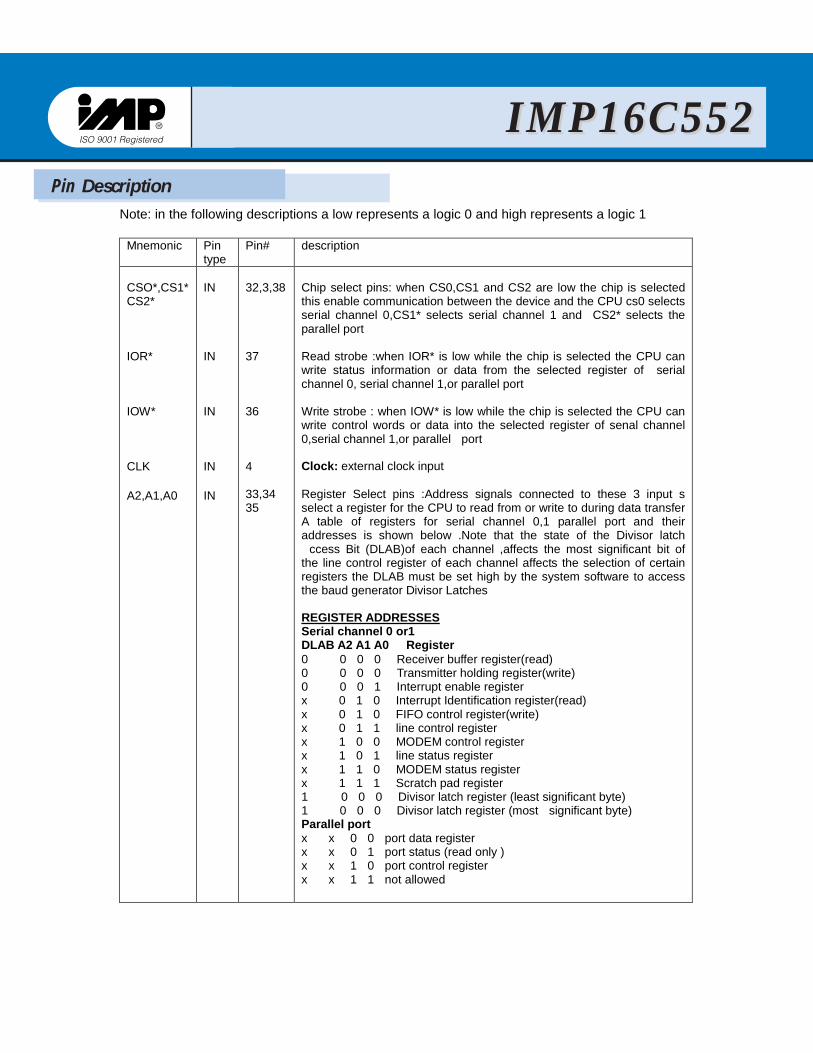
Note: in the following descriptions a low represents a logic 0 and high represents a logic 1
Mnemonic Pin type
Pin# description
CSO*,CS1* CS2* IOR* IOW* CLK A2,A1,A0
IN IN IN IN IN
32,3,38 37 36 4 33,34 35
Chip select pins: when CS0,CS1 and CS2 are low the chip is selected this enable communication between the device and the CPU cs0 selects serial channel 0,CS1* selects serial channel 1 and CS2* selects the parallel port Read strobe :when IOR* is low while the chip is selected the CPU can write status information or data from the selected register of serial channel 0, serial channel 1,or parallel port Write strobe : when IOW* is low while the chip is selected the CPU can write control words or data into the selected register of senal channel 0,serial channel 1,or parallel port Clock: external clock input Register Select pins :Address signals connected to these 3 input s select a register for the CPU to read from or write to during data transfer A table of registers for serial channel 0,1 parallel port and their addresses is shown below .Note that the state of the Divisor latch Access Bit (DLAB)of each channel ,affects the most significant bit of the line control register of each channel affects the selection of certain registers the DLAB must be set high by the system software to access the baud generator Divisor Latches REGISTER ADDRESSES Serial channel 0 or1 DLAB A2 A1 A0 Register 0 0 0 0 Receiver buffer register(read) 0 0 0 0 Transmitter holding register(write) 0 0 0 1 Interrupt enable register x 0 1 0 Interrupt Identification register(read) x 0 1 0 FIFO control register(write) x 0 1 1 line control register x 1 0 0 MODEM control register x 1 0 1 line status register x 1 1 0 MODEM status register x 1 1 1 Scratch pad register 1 0 0 0 Divisor latch register (least significant byte) 1 0 0 0 Divisor latch register (most significant byte) Parallel port x x 0 0 port data register x x 0 1 port status (read only ) x x 1 0 port control register x x 1 1 not allowed
4 408-432-9100/www.impweb.com © 2002 IMP, Inc.
Pin Description
IMP16C552IMP16C552

Mnemonic Pin type
Pin# description
RESET SIN0 STS1 DSR0*, DSR1* DSR0* DSR1* RLSD0* RISD1* RI0* RI1* VCC VSS
IN IN IN IN IN IN IN
39 41.62 28.13 31.5 29.8 30.6 23.40.64 2.7.27 43.54
Master reset: When this input is low it clears all the register(except the Receiver Buffer, Transfer Holding and Divisor Latches) and the control logic of the both channels and parallel port the states of various output signals are affected by an active RESET input (refer to table 1) .this input is buffered with a TTL-compatible schmitt trigger with 0.5v hysteresis. Serial inputs :Serial data input from the communication link such as peripheral device , MODE or data set to the associated serial channel Clear To Send: When low this pin indicates that the MODEM or data set is ready to exchange data The CTS0(1)*.signal is a MODEM status input whose conditions can be tested by the CPU reading bit4(CTS)of the MODEM Status Register Bit4 is the complement of the CTS0(1) signal Bit 0 (DCTS )of the MODEM status register indicates whether the CTS(1)* input has changed state since the previous reading of the modem status register CTS0(1)* has no the Transmitter Note: whenever the CTS bit of the MODEM status register changes state an interrupt is generated if the MODEM status interrupt is enabled Data Set Ready :When low this pin indicates that modem or data set is ready to establish the communication link with the UART the DSR0(1) signal is a MODEM status input whose condition can be tested by the CPU reading bit 5 (DSR)of the MODEM status register bit 5 is the complement of the DSR0(1)* signal. bit 1 (DDSR) of the MODEM Status Register Indicates whether the DSR0(1)* input has changed state since the previous reading of the MODEM Status Register DSR0(1)* has no the transmitter Note: Whenever the DSR bit of the MODEM Status Register changes state, an interrupt is generated if the MODEM status interrupt is enable Receiver Line Signal Detect: When low ,this pin indicates that the data canter has been detected by the MODEM or data set The RLSD0(1)* signal is a MODEM status input whose condition can be tested by the CPU reading bit 7(RLSD)of the MODEM Status Register Bit 7 is the complement of the RLSD0(1)* signal. Bit 3 (DRLSD) of the MODEM Status Register indicates whether the RLSD0(1)* input has changed state since the previous reading of the MODEM Status Register RLSD0(1)* has no effect on the receive Note: whenever the RLSD bit of the MODE status register changes state on interrupt is generated if the MODEM status interrupt is enable Ring indicator : when low this pin indicates that a telephone ringing signal has been received by the MODEM or data set The RI0(1)* signal is a MODEM status input whose condition can be tested by the CPU reading bit 6 (RI) of the MODEM Status Register Bit 6 is the complement of the RI0(1) signal Bit2 (TERI) of MODEM Status Register indicates whether the RI0(1) input signal has changed from a low to a high state since the previous reading of the MODEM Status Register. Note: whenever the RI bit of the MODEM Status Register changes from a low to a high state an interrupt is generated if the MODEM status interrupt is enabled +5V supply Ground
5 408-432-9100/www.impweb.com © 2002 IMP, Inc.
IMP16C552IMP16C552

Mnemonic Pin
type Pin# Description
DTR0* DTR1* RTS0* RTS1* TXRdy0* TXRDy1* Rxrdy0* RXRdy1 BDO
OUT OUT OUT OUT OUT
25,11 24,12 22,42 9,61 44
Data Terminal Ready :When low this informs the MODEM or data set that the UART is ready to establish a communication link The DTR0(1)* output signal can be set to an active low by programming bit 0 (DTR) of the MODEM Control Register to a 1.A Master reset operation sets this inactive (high) state. Loop mode operation holds this signal in its inactive state Request To Send: When low this informs the MODEM or data set that the UART is ready to exchange data. The RTS0(1)* output signal can be set to an active low by programming bit 1 (RTS)of the MODEM Control register to a 1.A Master Reset operation sets this signal to its inactive (high) state . Loop operation holds this signal in its inactive state Transmitter Ready pins: Transmitter DMA signalling is available through this pin for each serial channel When operating in the FIFO mode one of two types of DMA signaling can be selected via FCR3. When operating as in the Character Mode, only DMA mode 0is allowed. Mode 0 supports single transfer multi-transfer DMA where multiple transfers are made continuously until the XMIT FIFO has been filled TXRDY mode 0:when in non FIFO mode (FCR3=1) or in the FIFO mode (FCR0=1,FCR3=0) there are no characters in the XMIT FIFO or XMIT holding register the TXRDY pin will be low active . once it is activated the TXRDY0 TXRDY1.pin will go inactive after the first character is loaded into the XMIT FIFO or holding register TXRDY MODE 1:In the FIFO Mode (FCR0=1,FCR3=1)if there is at least one untilled position in the XMIT FIFO, it will go low active. This pin will become inactive when the XMIT FIFO is completely full Receiver Ready pins: Receiver DMA signaling is available through this pin when operating in the FIFO mode one of two types of DMA signaling can be selected via FCR3. When operating as in the Character Mode, only DMA mode O is allowed Mode 0supports single transfer DMA where a transfer is made between CPU bus cycles Mode 1 supports multiple transfers DMA where multiple transfer are made continuously until the RCVR FIFO has been emptied RXRDY Mode 0: When in the FI FO Mode (FCR=0)or in the FIFO Mode (FCR0=1.FCR3=0)there is at least 1 character in the RCVR FIFO or RCVR holding register the RXRDY0*, RXRDY1* pin will go low active, Once it is activated the RXRDY0*, RXRDY1* pin will go inactive when there are no more characters in the FIFO or holding register RXRDY MODE 1: in the FIFO mode (FCR0=1,FCR3=1 ) the trigger level or the timeout has been reached, the RXRDY0*, RXRDY1* pin will go low active. Once it is activated it will go inactive when there are no more characters in the FIFO or holding register. Bus Buffer Output :This goes high whenever the CPU is reading data or status from either the serial channel or parallel port It can be used to disable or control direction of a data bus transceiver between the CPU and the device.
6 408-432-9100/www.impweb.com © 2002 IMP, Inc.
IMP16C552IMP16C552
Mnemonic Pin
type Pin# description
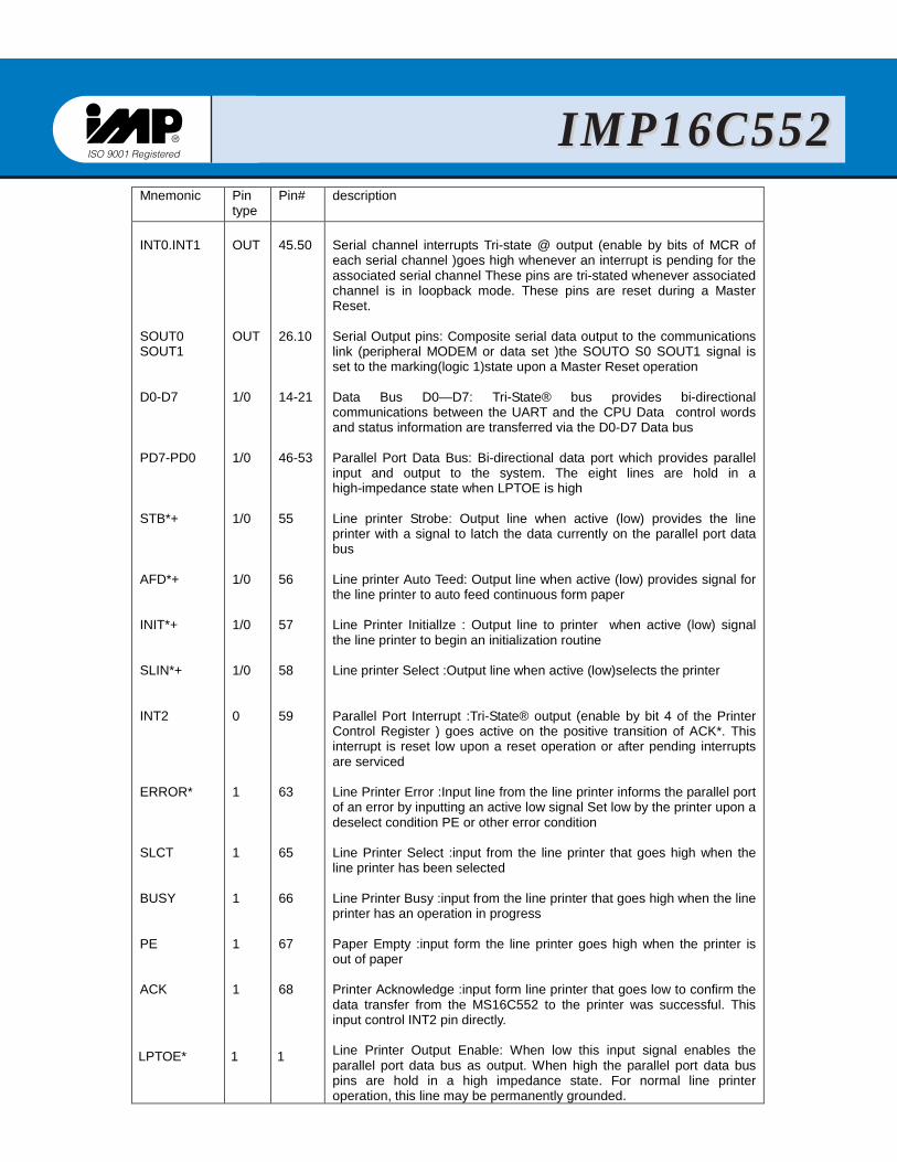
INT0.INT1 SOUT0 SOUT1 D0-D7 PD7-PD0 STB*+ AFD*+ INIT*+ SLIN*+ INT2 ERROR* SLCT BUSY PE ACK
OUT OUT 1/0 1/0 1/0 1/0 1/0 1/0 0 1 1 1 1 1
45.50 26.10 14-21 46-53 55 56 57 58 59 63 65 66 67 68
Serial channel interrupts Tri-state @ output (enable by bits of MCR of each serial channel )goes high whenever an interrupt is pending for the associated serial channel These pins are tri-stated whenever associated channel is in loopback mode. These pins are reset during a Master Reset. Serial Output pins: Composite serial data output to the communications link (peripheral MODEM or data set )the SOUTO S0 SOUT1 signal is set to the marking(logic 1)state upon a Master Reset operation Data Bus D0—D7: Tri-State® bus provides bi-directional communications between the UART and the CPU Data control words and status information are transferred via the D0-D7 Data bus Parallel Port Data Bus: Bi-directional data port which provides parallel input and output to the system. The eight lines are hold in a high-impedance state when LPTOE is high Line printer Strobe: Output line when active (low) provides the line printer with a signal to latch the data currently on the parallel port data bus Line printer Auto Teed: Output line when active (low) provides signal for the line printer to auto feed continuous form paper Line Printer Initiallze : Output line to printer when active (low) signal the line printer to begin an initialization routine Line printer Select :Output line when active (low)selects the printer Parallel Port Interrupt :Tri-State® output (enable by bit 4 of the Printer Control Register ) goes active on the positive transition of ACK*. This interrupt is reset low upon a reset operation or after pending interrupts are serviced Line Printer Error :Input line from the line printer informs the parallel port of an error by inputting an active low signal Set low by the printer upon a deselect condition PE or other error condition Line Printer Select :input from the line printer that goes high when the line printer has been selected Line Printer Busy :input from the line printer that goes high when the line printer has an operation in progress Paper Empty :input form the line printer goes high when the printer is out of paper Printer Acknowledge :input form line printer that goes low to confirm the data transfer from the MS16C552 to the printer was successful. This input control INT2 pin directly. Line Printer Output Enable: When low this input signal enables the parallel port data bus as output. When high the parallel port data bus pins are hold in a high impedance state. For normal line printer operation, this line may be permanently grounded.
7 408-432-9100/www.impweb.com © 2002 IMP, Inc.
LPTOE* 1 1
IMP16C552IMP16C552
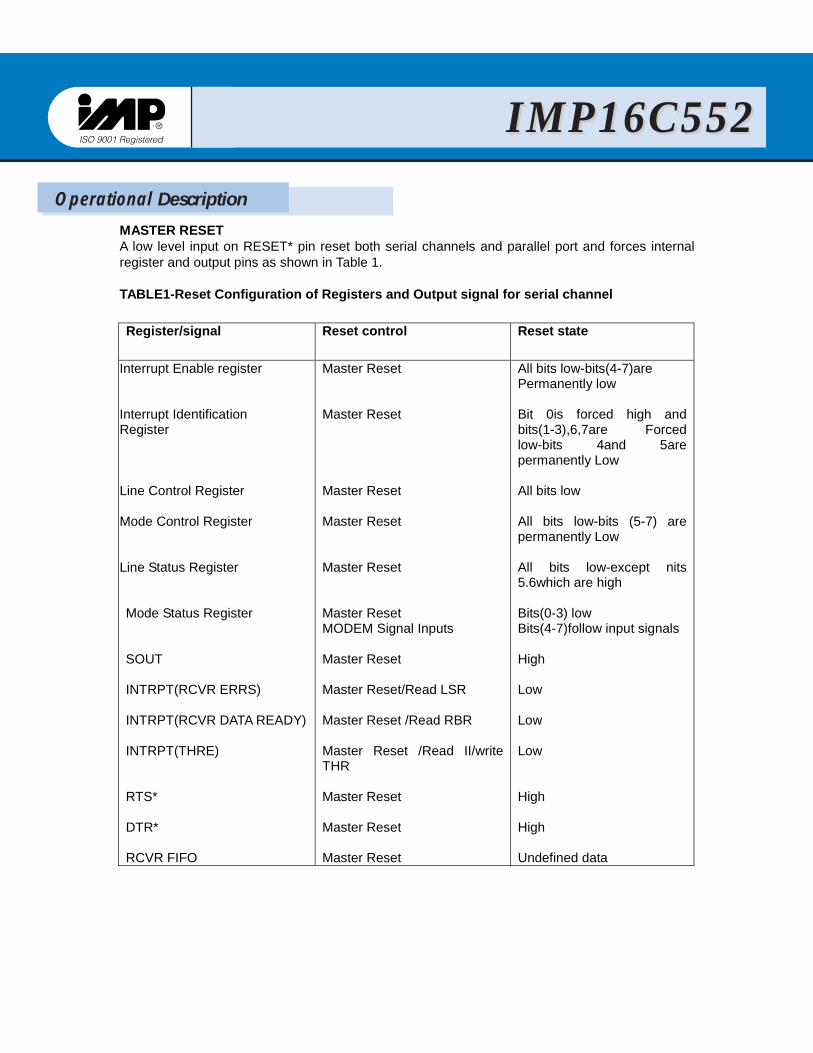
MASTER RESET A low level input on RESET* pin reset both serial channels and parallel port and forces internal register and output pins as shown in Table 1. TABLE1-Reset Configuration of Registers and Output signal for serial channel Register/signal Reset control Reset state
Interrupt Enable register Interrupt Identification Register Line Control Register Mode Control Register Line Status Register Mode Status Register SOUT INTRPT(RCVR ERRS) INTRPT(RCVR DATA READY) INTRPT(THRE) RTS* DTR* RCVR FIFO
Master Reset Master Reset Master Reset Master Reset Master Reset Master Reset MODEM Signal Inputs Master Reset Master Reset/Read LSR Master Reset /Read RBR Master Reset /Read II/write THR Master Reset Master Reset Master Reset
All bits low-bits(4-7)are Permanently low Bit 0is forced high and bits(1-3),6,7are Forced low-bits 4and 5are permanently Low All bits low All bits low-bits (5-7) are permanently Low All bits low-except nits 5.6which are high Bits(0-3) low Bits(4-7)follow input signals High Low Low Low High High Undefined data
8 408-432-9100/www.impweb.com © 2002 IMP, Inc.
Operational Description
IMP16C552IMP16C552
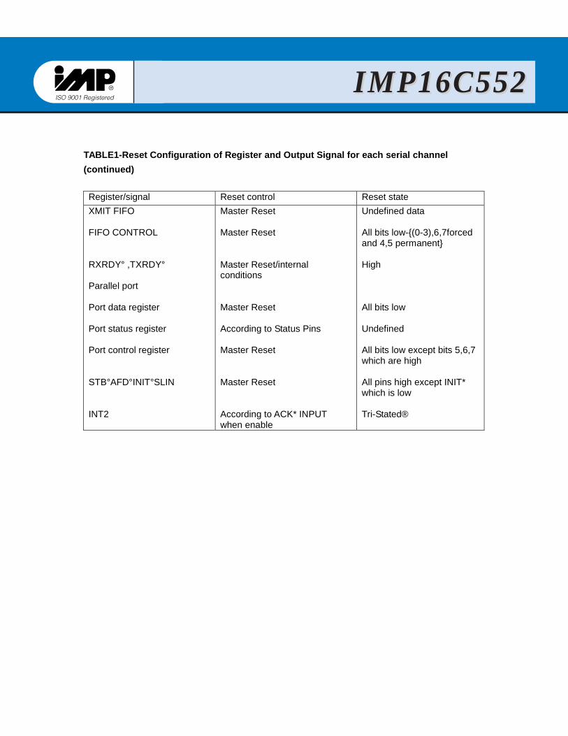
TABLE1-Reset Configuration of Register and Output Signal for each serial channel (continued) Register/signal Reset control Reset state XMIT FIFO FIFO CONTROL RXRDY° ,TXRDY° Parallel port Port data register Port status register Port control register STB°AFD°INIT°SLIN INT2
Master Reset Master Reset Master Reset/internal conditions Master Reset According to Status Pins Master Reset Master Reset According to ACK* INPUT when enable
Undefined data All bits low-{(0-3),6,7forced and 4,5 permanent} High All bits low Undefined All bits low except bits 5,6,7 which are high All pins high except INIT* which is low Tri-Stated®
9 408-432-9100/www.impweb.com © 2002 IMP, Inc.
IMP16C552IMP16C552
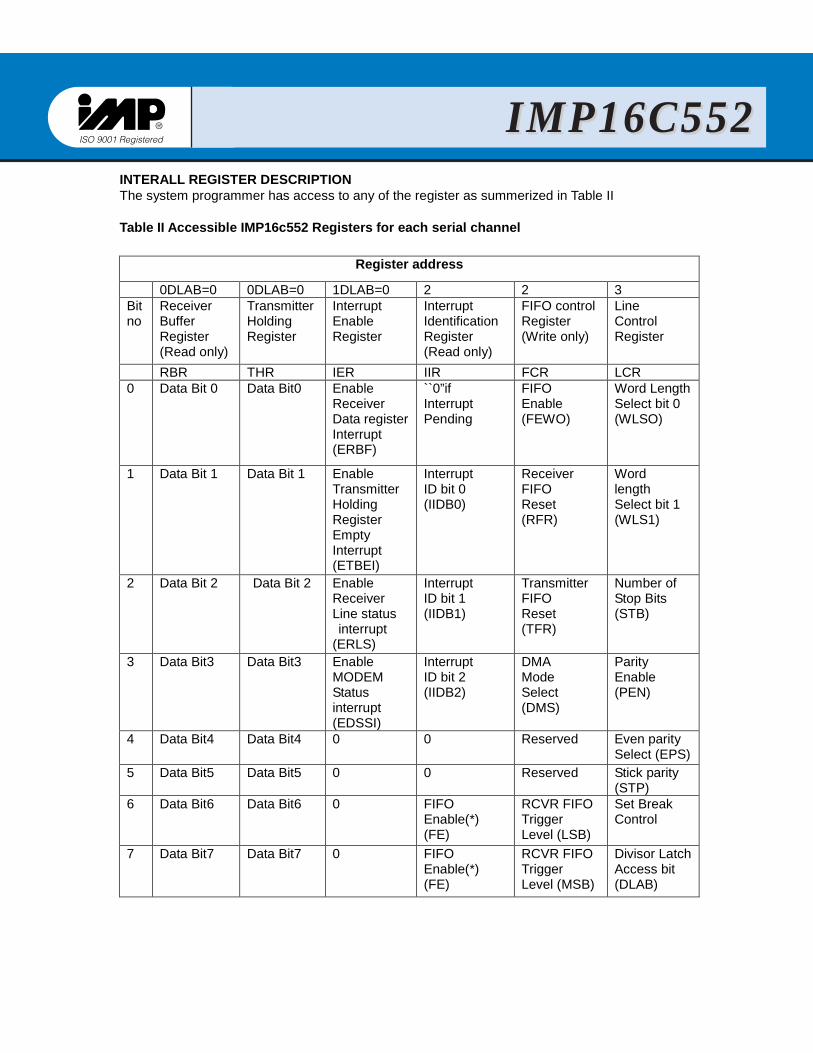
INTERALL REGISTER DESCRIPTION The system programmer has access to any of the register as summerized in Table II Table II Accessible IMP16c552 Registers for each serial channel
Register address
0DLAB=0 0DLAB=0 1DLAB=0 2 2 3 Bit no
Receiver Buffer Register (Read only)
Transmitter Holding Register
Interrupt Enable Register
Interrupt Identification Register (Read only)
FIFO control Register (Write only)
Line Control Register
RBR THR IER IIR FCR LCR 0 Data Bit 0 Data Bit0 Enable
Receiver Data register Interrupt (ERBF)
``0”if Interrupt Pending
FIFO Enable (FEWO)
Word Length Select bit 0 (WLSO)
1 Data Bit 1 Data Bit 1 Enable Transmitter Holding Register Empty Interrupt (ETBEI)
Interrupt ID bit 0 (IIDB0)
Receiver FIFO Reset (RFR)
Word length Select bit 1 (WLS1)
2 Data Bit 2 Data Bit 2 Enable Receiver Line status interrupt (ERLS)
Interrupt ID bit 1 (IIDB1)
Transmitter FIFO Reset (TFR)
Number of Stop Bits (STB)
3 Data Bit3 Data Bit3 Enable MODEM Status interrupt (EDSSI)
Interrupt ID bit 2 (IIDB2)
DMA Mode Select (DMS)
Parity Enable (PEN)
4 Data Bit4 Data Bit4 0 0 Reserved Even parity Select (EPS)
5 Data Bit5 Data Bit5 0 0 Reserved Stick parity (STP)
6
Data Bit6 Data Bit6 0 FIFO Enable(*) (FE)
RCVR FIFO Trigger Level (LSB)
Set Break Control
7
Data Bit7 Data Bit7 0 FIFO Enable(*) (FE)
RCVR FIFO Trigger Level (MSB)
Divisor Latch Access bit (DLAB)
10 408-432-9100/www.impweb.com © 2002 IMP, Inc.
IMP16C552IMP16C552

Table II Accessible IM16c552 Registers for each serial channel
Register address
4 5 6 7 0DLAB=1 1DLAB=1 Bit no
MODEM Control Register
Line status Register (read only)
MODEM Status Register
Scratch Pad Register
Divisor Latch (LSB)
Divisor Latch (MSB)
MCR LSR MSR SCR DLL DLM 0 Data
Terminal Read (RTS)
Data Ready (DR)
Delta Clear to Send (DCTS)
Bit 0 Bit 0 Bit 8
1 Request to send (RTS)
Overrun Error (OE)
Delta Data set Ready (DDSR)
Bit 1 Bit 1 Bit 9
2
Cut 1 Parity Error (PE)
Trailing Edge Ring Indicator (TERI)
Bit 2 Bit 2 Bit 10
3
Out 2 (INTE)
Framing Error (FE)
Delta Receiver Line Detect (DRLSD)
Bit 3 Bit 3 Bit 11
4 Loop Break Interrupt (BI)
Clear to Send (CTS)
Bit 4 Bit 4 Bit 12
5 0 Transmitter Holding Register Empty (THRE)
Data Set Ready (DSR)
Bit 5 Bit 5 Bit 13
6 0 Transmitter Empty (TEMT)
Ring Indicator (RI)
Bit 6 Bit 6 Bit 14
7 0 Error in RCVR FIFO(``) (EIRF)
Receive Line Signal Detect (RLSD)
Bit 7 Bit 7 Bit 15
(*) These bits are read 0 in Character Mode of IMP16C552
11 408-432-9100/www.impweb.com © 2002 IMP, Inc.
IMP16C552IMP16C552

Line Control Register The system programmer specifies the format of the asynchronous data communications exchange and sets the divisor latch access bit via the line control register (LCR) the programmer can also read the contents of the line control register the read capability simplifies system programming and eliminates the need for separate storage in system memory of the line characteristics Bits 0 and1 : these two bit s specify the number of bits each transmitted or serial character the encoding of bits 0and 1 is as follows:
Bit 1 Bit 0 Character length
0 0 1 1
0 1 0 1
5bits 6bits 7bits 8bits
Bit 2: this bit specifies the number of stop bits transmitted and received in each serial character if bit 2is a logic 0 0ne stop bit is generated in the transmitted data if bit 2 is logic 1 when a 5-bit word length is selected via bits 0 and1 ,0ne and half stop bits are generated if bit 2 is a logic 1 when either a 6-7- ,or 8-bit word length is selected .2 stop bits are generated the receiver checks the fist stop-bit only regardless of the number of stop bits selected Bit3:this bit is the parity enable bit when bits 3 is a logic 1 a parity bit is generated (transmit data)or checked (receive data )between the last data word bit and stop bit of the serial data (the parity bit is used to produce an ever or odd number of 1’s when the data word bits and the parity bit are summed Bit 4:this bit is the even parity selects bit when bit 3 is a logic 1 and bit 4 is a logic 0 an odd number of logic 1 ‘s is transmitted or checked in the data word bits and parity bit when bit 3 is a logic 1 and bit 4 is a logic 1 and even number of logic 1s is transmitted or checked in the data word bits and parity bit Bit 5: this bit is the stick parity bit when bits 3 and 5 are logic 1 the parity bit is transmitted and detected by the receiver in the opposite state indicated by bit 4 is bit 5 is zero stick parity is disabled
Bit 6:thus bit is the break control bit it causes a break control condition to be transmitted to the receiving UART when bit 6 set to a logic 1 the serial output (SOUT) is forced to the spacing (logic0) state and remains there until bit 6 is set to a logic 0 this bit acts only on SOUT pin and has no effect on transmitted logic this feature enable the CPU to alert a terminal in a computer communications system if the following sequence is followed no erroneous characters will be transmission because of break. 1 .Load an all 0s pad character in response to THRE 2. set break after the next THER 3. wait for the transmitted to be idle (TEMT=1) and clear break when normal transmitted has to be restored During the break the transmitted can be the used as a character time to accurately establish the break duration Bit 7:this bit the divisor latch access bit (DLAB) it must be set high (logic1)to access the divisor latches of the baud rate generator during a read or write operation it must be set low (logic 0) to access the receiver buffer the transmitter holding register or the interrupt enable register Programmable baud rate generator The UART contains a programmable baud generator that is capable of taking any clock input from DC to 8 0 MHz and dividing it by any divisor from 1 to 2 � –1 the output frequency of the baud generator is 16 x the baud rate two 8-bit latches store the divisor in a 16-bit binary format. These Divisor Latches must be loaded during initialization to ensure proper operation of the Baud Rate Generator. Upon loading either of the Divisor Latches, a 16-bit Baud counter is immediately loaded. This prevents long counts on initial load. Table III. IV and V illustrate the use of the Baud Rate Generator with three different driving frequencies. Table III references to a 1.8430 MHz clock, table IV to a 3.070 MHz clock, and table V to a 8 MHz clock. For baud rates of 38400 and below, the error obtained is minimal. The accuracy of the desired baud rate is dependent on the crystal frequency chosen. Using a divisor of zero is not recommended. In no case should the data rate be greater than 512K baud.
12 408-432-9100/www.impweb.com © 2002 IMP, Inc.
IMP16C552IMP16C552
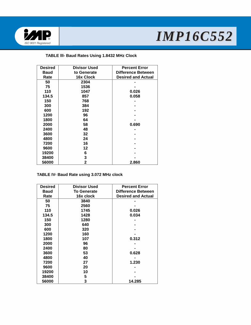
TABLE lll- Baud Rates Using 1.8432 MHz Clock
Desired
Baud Rate
Divisor Used to Generate 16x Clock
Percent Error Difference Between Desired and Actual
50 75 110
134.5 150 300 600 1200 1800 2000 2400 3600 4800 7200 9600 19200 38400 56000
2304 1536 1047 857 768 384 192 96 64 58 48 32 24 16 12 6 3 2
- -
0.026 0.058
- - - - -
0.690 - - - - - - -
2.860 TABLE IV- Baud Rate using 3.072 MHz clock
Desired Baud Rate
Divisor Used To Generate
16x clock
Percent Error Difference Between Desired and Actual
50 75 110
134.5 150 300 600 1200 1800 2000 2400 3600 4800 7200 9600 19200 38400 56000
3840 2560 1745 1428 1280 640 320 160 107 96 80 53 40 27 20 10 5 3
- -
0.026 0.034
- - - -
0.312 - -
0.628 -
1.230 - - -
14.285
13 408-432-9100/www.impweb.com © 2002 IMP, Inc.
IMP16C552IMP16C552

Table V- Baud Rate using 8.0 MHz Clock
Desired Baud Rate
Divisor Used To Generate
16x clock
Percent Error Difference Between Desired and Actual
50 75 110
134.5 150 300 600 1200 1800 2000 2400 3600 4800 7200 9600 19200 38400 56000 128000 256000
10000 6667 4545 3717 3333 1667 833 417 277 250 208 139 104 69 52 26 13 9 4 2
- 0.005 0.010 0.013 0.010 0.020 0.040 0.080 0.080
– 1.160 0.080 1.160 0.644 1.160 1.160 1.160 0.790 2.344 2.344
Line Status Register This register provides status information to the CPU concerning the data transfer. Table II shows the contents of the Line Status Register. Description of each bit follows: Bit 0: This bit is the receiver Data Ready (RDR) indicator. Bit 0 is set to a logic 1 whenever a complete incoming character has been received and transferred into the Receive Buffer Register of the FIFO. Bit 0 is reset to a logic 0 by reading all of the data in the Receive Buffer Register (for character mode ) or the RCVR FIFO (for FIFO mode). Bit 1: This bit is the Overrun Error (OE) indicator. Bit 1 indicates that data in the Receiver Buffer Register was not read by the CPU before the next character was transferred into the Receiver Buffer Register, thereby destroying the previous character. The OE indicator is set to a logic 1 upon detection of an overrun condition and reset whenever the CPU reads the contents of the Line Status Register. If the FIFO mode data continues to fill FIFO beyond the trigger level.
an overrun error will occur only after the FIFO is full and the next character has been completely received in the shift register. An OE is indicated as soon as it happens . The character in the shift register is overwritten, but nothing will transferred to the FIFO. Bit 2: This bit is the Parity Error (PE) indicator. Bit 2 indicates that the received data character does not have the correct even or odd parity, as selected by the even-parity-select bit. The PE is set to a logic 1 upon detection of a parity error and is reset to a logic 0 whenever the CPU reads the contents of the Line Status Register. In the FIFO mode this error is associated with the particular character in the FIFO and revealed to the CPU when the associated character is the top of the FIFO. Bit 3: This bit is the Framing Error (FE) indicator. Bit 3 indicates that the received character did not have a valid Stop bit. Bit 3 is set to a logic 1 whenever the Stop bit following the last data bit or parity bit is detected as a logic 0 bit (Spacing level). The FE indicator is reset whenever the CPU reads the contents of the Line Status Register. In the FIFO mode
14 408-432-9100/www.impweb.com © 2002 IMP, Inc.
IMP16C552IMP16C552
this error is associated with the particular character in the FIFO it applies to. This error is revealed to the CPU when its associated character is at the top of the FIFO. The UART will resynchronize after a Framing Error. Bits 4: This bit is the Break Interrupt (BI) indicator. Bit 4 is set to a logic 1 whenever the received data input is held in the spacing (logic 0 ) state for longer than a full word transmission time (that is, the total time of Start bit + data bits + Parity + Stop bits ). The BI indicator is reset whenever the CPU reads the contents of the Line Status Register. When in FIFO mode, BI is associated to the particular character in the FIFO, and this bit is set when the associated character is at the top of the FIFO. When a break occurs, only one zero character is loaded into the FIFO. The next character transferred is enable after SIN goes to the marking state (logic 1 ) and receives the next valid start bit. Note: Bits 1 through 4 are the error conditions that produce a Receiver Line Status interrupt whenever any of the corresponding conditions are detected and the interrupt enabled. Bit 5: This is the Transmitter Holding Register empty (THRE) indicator. Bit 5 indicates that the UART is ready to accept a new character for transmission. In addition, this bit causes the UART to issue an interrupt to the CPU when the Transmit Holding Register Empty Interrupt enable is set high. The THRE bit is set to a logic 1 when a character is transferred from the Transmitter Holding Register into the Transmitter Shift Register. The bit is reset to logic 0 concurrently with the loading of the Transmitter Holding Register by the CPU. In the FIFO mode, this bit will be set when XMIT FIFO is empty, and cleared when as least one character is written to XMIT FIFO. Bit 6: This bit is the Transmitter Empty (TEMT) indicator. Bit 6 is set to a logic 1 whenever the Transmitter Holding Register (THR) and the Transmitter Shift Register (TSR) are both empty. It is reset to a logic 0 whenever either the THR or the TSR contains a data character. In the FIFO mode this bit is set to 1 whenever the transmitter FIFO and
shift register are both empty. Bit 7 : In the Character Mode, this bit (LSR7) is a 0. In the FIFO mode it is set when there is a least one parity error, framing error or break indication in the FIFO. LSR7 is clear when the CPU reads the LSR, if there are no subsequent errors in the FIFO. Note: The Line Status Register is intended for read operations only. Writing to this register is not recommended. Interrupt Identification Register In order to provide minimum software overhead during data character transfers, the UART prioritizes interrupts into four levels and records these in the interrupt Identification Register. The four levels of interrupt conditions are as follows :Receiver Line Status (priority 1), Received Data Ready (priority 3 ) , and MODEM Status (priority 4). Information indicating that a prioritized interrupt is pending and source of that interrupt is stored in the Interrupt Identification Register (refer to Table VI). Register IIR. When addressed during chip select time, freezes the highest priority interrupt pending and no other interrupts are acknowledged until the particular interrupt is serviced by the CPU. Its contents are indicated in Table VI and are described below: Bit 0: This bit can be used in a prioritized or polled environment to indicate whether an interrupt is pending when bit 0 is a logic 0 an interrupt is pending and the IIR contents may be used as a pointer to the appropriate interrupts service routine when bit 0 is a logic 1 no interrupt is pending and polling (if used)continues Bit 1,2 : these two bits of IIR are used to identity the highest priority interrupt pending (see Table VI) Bit3 : In the character mode this bit 0 in the FIFO mode this bit is set along with bit 2 when a timeout interrupt is pending Bit 4,5: These two bits of the IIR are always logic 0
15 408-432-9100/www.impweb.com © 2002 IMP, Inc.
IMP16C552IMP16C552

TABLE VI- interrupt Control Functions Interrupt Identification Interrupt Set Reset Functions Register Bit3 Bit2 Bit1 Bit
0 Priority level
Interrupt type
Interrupt source Interrupt reset control
0 0 0 1 0 0
0 1 1 1 0 0
1 1 0 0 1 0
1 0 0 0 0 0
.— Highest second Second Third Fourth
None Receiver Line Status Received Data Available Character Timeout Identification (‘’) Transmitter Holding Register Empty MODEM Status
None Overrun error or party error or framing or break interrupt Receiver Data Available or Trigger Level Reached No characters have been input to or removed from the RCVR FIFO during the Last 4 character times, and there is at least one character in it during this time. Transmitter Holding Register Empty Clear to send or Data Set ready or Ring Indicator or Received Line Signal Detect
.--- Reading the Line Status Register Reading the Receiver Buffer Register or the FIFO Drops below the Trigger Level Reading the Receiver Buffer Register Reading the IIR Register (if source of interrupt) or Writing into the Transmitter Holding Register Reading the MODEM status Register
(*) This interrupt type is not available in character mode of IMP6C552.
16 408-432-9100/www.impweb.com © 2002 IMP, Inc.
IMP16C552IMP16C552

FIGURE 3 – Interrupt Control logic for channel 0 and 1
Bit 6, 7: These two bits, when set, indicate that the device is in FIFO Mode, i.e. when FCRO=1. Interrupt Enable Register This 8-bit register enables the four interrupt sources of the DUART to separately activate the chip Interrupt (INTRPT) output signal. Each interrupt can individually activate the interrupt (INTRPT) output signal. Its contents are indicated in Table 3-2 and are described below by resetting bits 0 through 3 of the interrupt Enable Register (IER). Similarly, setting bits of the IER register to a logic 1 enables the selected interrupt (s). Disabling an interrupt prevents it from being indicated as active in the IIR and from activating the INTRPT output signal. All other system functions operated in their normal manner, including the setting of the Line Status and MODE Status Registers. Bit 0: This bit enables the Received Data Available Interrupt (and timeout interrupt in the FIFO mode) when set to logic 1. Bit 1: This bit enables the Transmitter Holding Register Empty Interrupt when set to logic 1. Bit 2: This bit enables the Receiver Line Status Interrupt when set to logic 1. Bit 3: This bit enables the MODEM Status Interrupt when set to logic 1.
Bit 4-7: These four bits are always logic 0. Scratch Pad Register This 8-bit Read/Write Register does not control the UART in anyway. It is intended as a scratch pad register to be used by the programmer to hold general purpose data temporarily. FIFO Control Register This write only register is located at the same address as the IIR (read only). This register is used to enable FIFO Mode, clear FIFO’s, set the RCVR FIFO trigger levels, and select the mode of DMA signaling. Bit 0: Writing a 1 to this bit enables both the XMIT and RCVR FIFO’s. When changing from FIFO Mode to Character Mode and vice versa, data is not automatically cleared from the FIFO’s. This bit must be a 1 when writing to other FCR bits or they will not be programmed. Bit 1: Writing a 1 to FCR1 will reset its counters to 0, and then self clear this bit to 0. The shift register is not cleared. Bit 2: Functions the same as bit 1, except for XMIT FIFO counters. Bit 3: If FCR0=1, setting FCR# to a 1 will cause the RXRDY and TXRDY pins to change from mode 0 to mode 1 (see description of RXRDY and TXRDY pins).
INT0/1
RCVR line Status Interrupt 0/1RCVR Data Status Interrupt 0/1
RCVR Timout Status Interrupt 0/1THRE Interrupt 0/1
MODEM status interrupt 0/1
LOOPBACK enable(MCR0/1 bit4)
Internal OUTPUT2(MCR0/1 bit 3)
17 408-432-9100/www.impweb.com © 2002 IMP, Inc.
IMP16C552IMP16C552

Bit 4, 5: FCR 4 and FCR5 are reserved for future use. Bit 6,7: FCR6 and FCR7 are used to set the trigger level for the RCVR FIFO interrupt as follows:
7 6 RCVR FIFO Trigger Level (In bytes)
0 0 1 1
0 1 0 1
01 04 08 14
MODEM Control Register This 8-bit register controls the interface with the MODEM or data set (or a peripheral device emulating a MODEM ). The contents of the MODEM Control Register are indicated in Table II and are described below: Bit 0: This bit controls the Data Terminal Ready (DTR*) output. When bit 0 is set to a logic 1, DTR* output is forced to a logic 0. When bit 0 is reset to a logic 0, DTR* output is forced to a logic 1. Note: the DTR* output of the UART may be applied to an EIA inverting line driver (such as DS1488) to obtain the proper polarity input at the succeeding MODEM or data set. Bit 1: This bit controls the Request to Send (RTS*) output. Bit 1 affects the RTS* output in a manner identical to that bit 0 affects output DTR*. Bit 2: This bit controls the internal OUTPUT 1 signal, which is an auxiliary user-designated output. Bit 2 affects the OIUTPUT 1 in a manner identical to bit 0 affects output DTR*. Internal OUTPUT1 signal is not connected the external pin. Bit 3: This bit controls the internal OUTPUT2 signal, which is an auxiliary user-designated output. Bit 3 affects the OUT2* output in a manner identical to bit not connected to the external pin. When set, this bit enables INT2 pin internally. Bit 4: This bit provides a local loopback feature for diagnostic testing of the UART.
When bit 4 is set to logic 1, the following occur. The transmitter Serial Output (SOUT) is set to a logic 1 (high) state: the receiver Serial Input (SIN) is disconnected; the output of the Transmitter Shift Register is “looped back” into the Receiver Shift Register input: the four MODEM Control inputs (CTS*, DSR*. RLSD* and RI*) are disconnected. And the MODEM Control output pins (RST*, DTR*) are forced to their inactive state (high). In the diagnostic mode, data that is transmitted is immediately received. This feature allows the processor to verify the transmit-and receive-data paths of the UART. In the diagnostic mode, the receiver and transmitter interrupts are full operational. Their sources are external to the part. The MODEM control Interrupts are also operational, but the sources of interrupts are now the lower four bits of the MODEM Control Register instead of the four MODEM control inputs. The interrupts are still controlled by the Interrupt Enable Register. Bit 5-7: These bits are permanently set to logic 0. MODEM STATUS Register This 8-bit register provides the current state of the control lines from the MODEM or data set (or a peripheral device emulating a modem) to the CPU. In addition to this current-state information, four bits of the MODEM Status Register provide change information. These bits are set to a logic 1 whenever a control input from the MODEM changes state. They are reset to logic 0 whenever the CPU reads the MODEM Status Register. The contents of the MODEM Status Register are indicated in Table II and described below: Bit 0: This bit is the Delta Clear to Send (DCTS) indicator. Bit 0 when set to logic 1, indicates that the CTS* input to the chip has changed state since the last time it was read by the CPU. Bit 1: This bit is the Delta Data Set Ready (DDSR) indicator, Bit 1 when set to logic 1, indicates that the DSR input to the chip has
18 408-432-9100/www.impweb.com © 2002 IMP, Inc.
IMP16C552IMP16C552
changed state since the last time it was read by the CPU. Bit 2: This bit is the Trailing Edge of Rin Indicator (TREI) detector. Bit 2 indicates that the RI input to the chip has changed from a low to high state since the last time it was read by the CPU. Bit 3: This bit is the Delta Received Line Signal Detector (DRLSD) indicator. Bit 3 when set to logic 1, indicates that the RLSD input to the chip has changed state since the last time it was read by the CPU. Note: Whenever bit 0, 1, 2, or 3 is set to logic 1, a MODEM Status Interrupt is generated, if bit 3 (EDSSI) of the interrupt enable register is set. Bit 4: This bit is the complement of the Clear to Send (CTS*) input. This bit is equivalent to bit RTS of the MODEM control register, if bit 4 of the MCR is set to 1 (loop mode). Bit 5: This bit is the complement of the Data Set Ready (DSR)* input. This bit is equivalent to bit DTR of the MODEM control register, if bit 4 of the MCR is set to 1(loop mode). Bit 6: This bit is the complement of the Ring Indicator (RI)* input. This bit is equivalent to bit OUT1 of the MODEM control register, if bit 4 the MCR is set to 1 (loop mode). Bit 7: This bit is the complement of the Received Line Signal Detect (RLSD) input. This bit equivalent to bit OUT2 of the MODEM control register, if bit 4 of the MCR is set to 1 (loop mode). FIFO Interrupt Mode Operation When the RCVR FIFO and receiver interrupts are enabled, (FCR0=1, IER0=1) RCVR interrupts will occur as follows: A. The receive data available interrupt will
be issued to the CPU when the FIFO has reached its programmed trigger level; it will be cleared as soon as the FIFO drops below its programmed
trigger level. B. The IIR receive data available indication
also occurs when the FIFO trigger level is reached, and like the interrupt, it is cleared when the FIFO drops below the trigger level.
C. The receiver line status interrupt
(IIR=06), as before, has higher priority than the received data available (IIR=04) interrupt.
D. The data ready bit (LSR bit 0) is set as
soon as a character is transferred from the shift register to the RCVR FIFO. It is reset when the FIFO is empty.
When RCVR FIFO and receiver interrupts are enabled, RCVR FIFO timeout interrupts will occur as follows: A. A FIFO timeout interrupt will occur, if the
following conditions exists: -at least one character is in the RCVR FIFO.
-the most recent serial character received was longer than 4 continuous character times ago (if 2 stop bits are programmed the second one is included in this time delay ).
-the most recent CPU read of the FIFO was longer than 4 continuous character times ago.
This will cause a maximum character received to interrupt issued delay of 160 ms at 300 BAUD with a 12 bit character. B. character times are calculated by using
the RCLK input for a clock signal (this makes the delay proportional to the baud rate).
C. When a timeout interrupt has occurred, it
is cleared and the timer is reset when the CPU reads one character form the RCVR FIFO.
D. When a timeout interrupt has not
occurred the ` timeout timer is reset after a new character is received or after the
19 408-432-9100/www.impweb.com © 2002 IMP, Inc.
IMP16C552IMP16C552

CPU reads the RCVR FIFO. When the XMIT FIFO and transmitter interrupts are enabled (FCR0=1, IER1=1), XMIT interrupts will occur as follows: A. The transmitter holding register interrupt
(02) occurs when the XMIT FIFO is empty; it is cleared as soon as the transmitter holding register is written to (1 to 16 characters may be written to this XMIT FIFO while servicing this interrupt) or the IIR is read.
B. The transmitter FIFO empty indications
will be delayed 1 character time minus the last stop bit time whenever the following occurs: THRE=1 and there have not been at least tow bytes at the same time in the transmit FIFO, since the last THRE=1, The first transmitter interrupt after changing FCR0 will be immediate, if it is enabled.
Character timeout and RCVR FIFO trigger level interrupts have the same priority as the current received data available interrupt; XMIT FIFO empty has the same priority as the current transmitter holding register empty interrupt. FIFO Polled Mode Operation
With FCR0=1 RESETTING IER1, IER2, IERR3 or all to zero puts the UART in the RCVR and XMITTER are controlled separately either one or both can be in the polled mode of operation. In this mode the users program will check RCVR and XMITTED status via the LSR. As stated previously: LSR0 will be set as long as there is one byte in the RCVR FIFO. LSR1 to LSR4 will specify which error(s) has occurred. Character error status is handled the same way as when in the interrupt mode, the IIR is not affected since IER2=0. LSR5 will indicate when the XMIT FIFO is empty. LSR6 will indicate that both the XMIT FIFO and shift register are empty. LSR7 will indicate whether there are any errors in the RCVR FIFO. There is no trigger level reached or timeout condition indicated in the FIFO Polled Mode. However, the RCVR and XMIT FIFO’s are still fully capable of holding characters.
20 408-432-9100/www.impweb.com © 2002 IMP, Inc.
IMP16C552IMP16C552
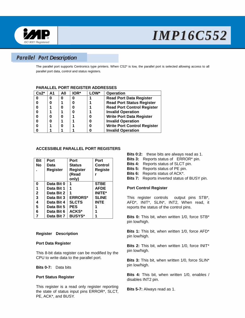
The parallel port supports Centronics type printers. When CS2* is low, the parallel port is selected allowing access to all parallel port data, control and status registers.
PARALLEL PORT REGISTER ADDRESSES Cs2* A1 A0 IOR* LOW* Operation 0 0 0 0 0 0 0 0
0 0 1 1 0 0 1 1
0 1 0 1 0 1 0 1
0 0 0 0 1 1 1 1
1 1 1 1 0 0 0 0
Read Port Data Register Read Port Status Register Read Port Control Register Invalid Operation Write Port Data Register Invalid Operation Write Port Control Register Invalid Operation
ACCESSIBLE PARALLEL PORT REGISTERS Bit No.
Port Data Register
Port Status Register (Read only)
Port Control Register
0 1 2 3 4 5 6 7
Data Bit 0 Data Bit 1 Data Bit 2 Data Bit 3 Data Bit 4 Data Bit 5 Data Bit 6 Data Bit 7
1 1 1 ERRORS* SLCTS PES ACKS* BUSYS*
STBE AFDE INITE* SLINE INTE 1 1 1
Register Description Port Data Register This 8-bit data register can be modified by the CPU to write data to the parallel port. Bits 0-7: Data bits Port Status Register This register is a read only register reporting the state of status input pins ERROR*, SLCT, PE, ACK*, and BUSY.
Bits 0:2: these bits are always read as 1. Bits 3: Reports status of ERROR* pin. Bits 4: Reports status of SLCT pin. Bits 5: Reports status of PE pin. Bits 6: Reports status of ACK*. Bits 7: Reports inverted status of BUSY pin. Port Control Register This register controls output pins STB*, AFD*, INIT*, SLIN*, INT2, When read, it reports the status of the control pins. Bits 0: This bit, when written 1/0, force STB* pin low/high. Bits 1: This bit, when written 1/0, force AFD* pin low/high. Bits 2: This bit, when written 1/0, force INIT* pin low/high. Bits 3: This bit, when written 1/0, force SLIN* pin low/high. Bits 4: This bit, when written 1/0, enables / disables INT2 pin. Bits 5-7: Always read as 1.
21 408-432-9100/www.impweb.com © 2002 IMP, Inc.
Parallel Port Description
IMP16C552IMP16C552
AC, DC TIMING SPECIFICATION Absolute Maximum Ratings Temperature Under Bias 00c to +700c Storage or Output Voltage –650c to + 1500c All Input or Output Voltages With Respect to VSS -0. 5 V to + 7. 0 V Power Dissipation 500 mw
If Military/Aerospace specified devices are required. contact Modular for availability and specifications. Note: Maximum rating indicate limits beyond which permanent damage may occur. Continuous operation at these limits is not intended and should be limited to those conditions specified under DC electrical characteristics.
DC ELECTRICAL CHARACTERISTICS TA=00C to + 700c, Vcc=+5V±5%, Vss=0V, unless otherwise specified Symbol Parameter Conditions Min Max Units VILX VIHX VIL VIH VOL VOH ICC(AV) IIL ICL LOZ VILMR VIHMR
Clock Input Low Voltage Clock Input High Voltage Input Low Voltage Input High Voltage Output Low Voltage Output High Voltage Avg. Power Supply Current(Vcc) Input Leakage Clock Leakage Tri-State® Leakage MR Schmitt VIL MR Schmitt VIH
IOL = 4.0 mA on D0-D7 = 12 mA on PD0-PD7
=10 mA on INT*, AFD*, STB*, SLIN*(note1) = 2mA on all other OUTPUTS
IOH = -1. 0 mA (note 1) = -2.0 mA on PD0-PD7 =-0.2 mA on INT*, AFD* STB*, SLIN* = -0.2mA on all other OUTPUTS Vcc =5. 25V, f=4MHz No Loads on outputs SIN, DSR, DCD All other inputs =0. 8V Vcc=5. 25V, Vss=0V All other pins floating VOUT = 0v, 5. 25v VCC=5. 25V, VSS=0V VOUT =0V, 5. 25V 1) chip deselected 2) WRITE mode, chip selected
-0. 5V 2. 0 -0. 5V 2. 0 2. 4 2. 0
0.8 Vcc 0.8 Vcc 0.4 10 ±10 ±10 ±10 0. 8
V V V V V V mA µA µA µA V V
22 408-432-9100/www.impweb.com © 2002 IMP, Inc.
IMP16C552IMP16C552
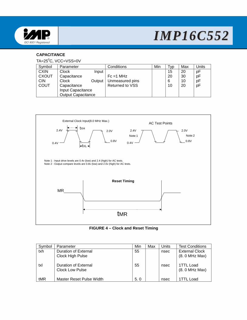
CAPACITANCE TA=250C, VCC=VSS=0V Symbol Parameter Conditions Min Typ Max Units CXIN CXOUT CIN COUT
Clock Input Capacitance Clock Output Capacitance Input Capacitance Output Capacitance
Fc =1 MHz Unmeasured pins Returned to VSS
15 20 6 10
20 30 10 20
pF pF pF pF
FIGURE 4 – Clock and Reset Timing Symbol Parameter Min Max Units Test Conditions txh txl tMR
Duration of External Clock High Pulse Duration of External Clock Low Pulse Master Reset Pulse Width
55 55 5. 0
nsec nsec nsec
External Clock (8. 0 MHz Max) 1TTL Load (8. 0 MHz Max) 1TTL Load
External Clock Input(8.0 MHz Max.)
tXH2.4V
0.4VtXL
2.0V
0.8V
2.4V
Note:1
0.4V
AC Test Points
2.0V
0.8V
Note:2
tMR
Reset Timing
Note 1 : Input drive levels are 0.4v (low) and 2.4 (high) for AC tests.Note 2 : Output compare levels are 0.8v (low) and 2.0v (high) for AC lests.
MR
23 408-432-9100/www.impweb.com © 2002 IMP, Inc.
IMP16C552IMP16C552
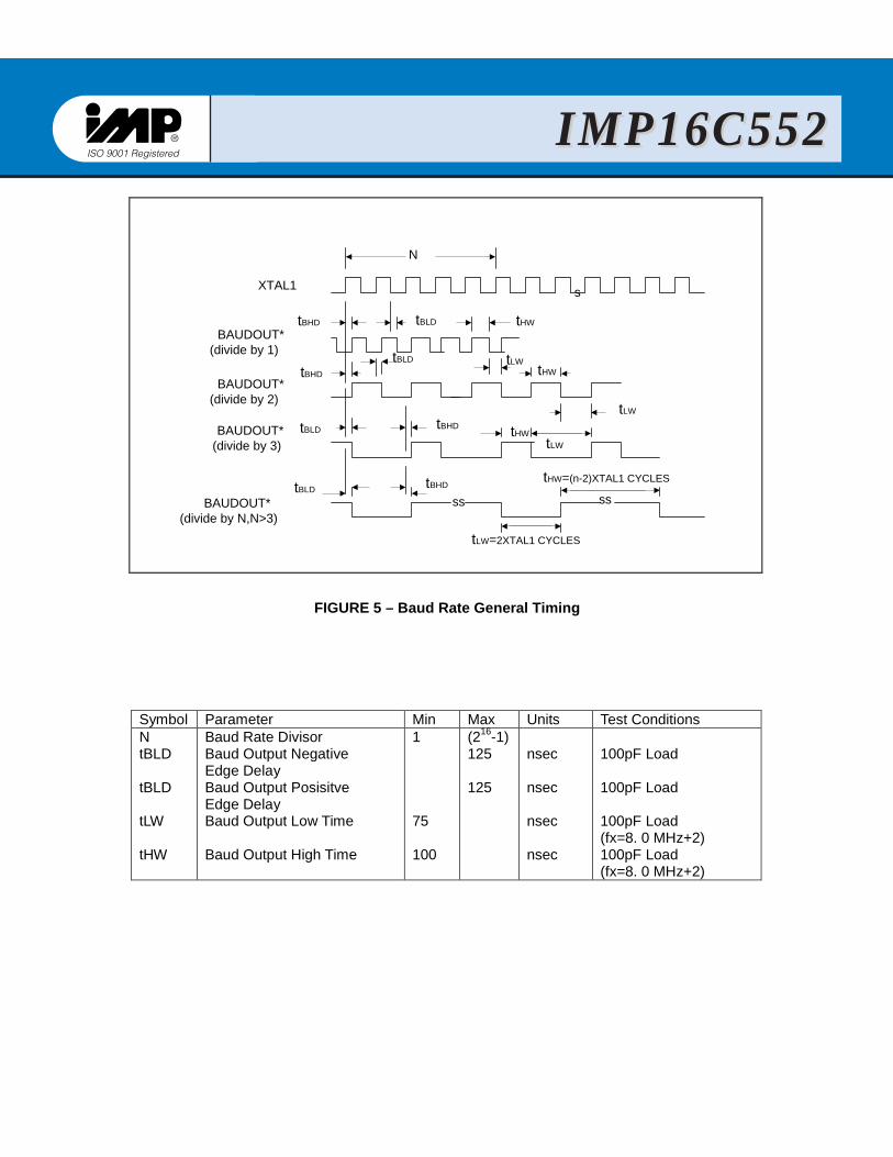
FIGURE 5 – Baud Rate General Timing
Symbol Parameter Min Max Units Test Conditions N tBLD tBLD tLW tHW
Baud Rate Divisor Baud Output Negative Edge Delay Baud Output Posisitve Edge Delay Baud Output Low Time Baud Output High Time
1 75 100
(216-1) 125 125
nsec nsec nsec nsec
100pF Load 100pF Load 100pF Load (fx=8. 0 MHz+2) 100pF Load (fx=8. 0 MHz+2)
s
ssss
N
tBLD tHW
tLW tHW
tBLD
tBHD
tBHD
tBLD tBHD tHW tLW
tBLD tBHD
tLW
tHW=(n-2)XTAL1 CYCLES
tLW=2XTAL1 CYCLES
XTAL1
BAUDOUT* (divide by 1)
BAUDOUT*(divide by 2)
BAUDOUT*(divide by 3)
BAUDOUT* (divide by N,N>3)
24 408-432-9100/www.impweb.com © 2002 IMP, Inc.
IMP16C552IMP16C552

FIGURE 6 – Write cycle Timing
FIGURE 7- Read Cycle Timing
VALID DATA
tDH tDD ACTIVE
ACTIVE
tWCWCtDOW
ACTIVE
tDOC
tDOCtACW
tACWVALIDA0,A1,A2
CS0*(CS1*)
IOW*
IOR*
DATAD0-D7
ACTIVE
ACTIVE
tRCRCtDIW
ACTIVE
tDIC
tDIC tACR
tACR
VALIDA0,A1,A2
CS0*(CS1*)
IOR*
IOW*
BD0
tDD tDD
VALID DATA
tHZ tDDDDATAD0-D7
25 408-432-9100/www.impweb.com © 2002 IMP, Inc.
IMP16C552IMP16C552

Symbol Parameter Min Max Units Test conditions TDIW RC tDD tDDD tHZ tDOW WC tDS tDH tDIC tDOC tACR tACW tWC tRC
IOR* Strobe Width Read Cycle(tDIC + tDIW + tRC) IOR* to Driver Enable/Disable Delay Delay from IOR* to Data IOR* to floating Data Delay IOW* Strobe Width Write Cycle (tDOC + tDOW + tWC) Data Setup Time Data Hold Time IOR* delay from chip Select or Address IOW* delay from chip Select or Address Address and Chip Select Hold time from IOR* Address and Chip Select Hold time from IOW* Write Cycle Delay Read Cycle Delay
50 105 0 0 50 110 15 15 25 25 2 2 60 50
60 40 100
nsec nsec nsec nsec nsec nsec nsec nsec nsec nsec nsec nesc nesc nesc nesc
1 TTL Load 1 TTL Load @100pF Load @100pF Load @100pF Load 1 TTL Load 1 TTL Load 1 TTL Load 1 TTL Load 1 TTL Load 1 TTL Load 1 TTL Load 1 TTL Load 1 TTL Load 1 TTL Load
26 408-432-9100/www.impweb.com © 2002 IMP, Inc.
IMP16C552IMP16C552

FIGURE 8 – Modem Control Timing
Symbol Parameter Min Max Units Test Conditions tMDO tSIM tRIM
Delay from IOW* (WR MCR) Delay to Set Interrupt From MODEM Input Delay to Reset Interrupt From IOR* (RD MSR)
200 200 30
nsec nsec nsec
100pF Load 100pF Load 100pF Load
tSIMtRIM tSIM tRIM
tSIM
tMDO tMDO
IOW*(1) (write MCR)
RIS*,DTR*
CTS*,DSR*,RLSD*
INT0
IOR*(2) (read MSR)
RI*
NOTES: (1)See Write cycle Timing (2)See Read cycle Timing
27 408-432-9100/www.impweb.com © 2002 IMP, Inc.
IMP16C552IMP16C552

FIGURE 9 – Receiver Timing
Symbol Parameter Min Max Units Test Conditions tSCD tSINT TrinT
Delay from RCLK To Sample Time Delay from Stop to Set Interrupt Delay From IOR* (RD RBR or RD LSR) Reset Interrupt
2 1(*) 32
µsec RCLK Cycles nsec
100pF Load
(*) When receiving the first byte in FIFO mode tSINT will be delayed 3 RCLK cycles, except for a timeout interrupt where tSINT will be delayed 8 RCLK cycles.
8 CLKS tSCD
START DATA BITS(5-8)
PARITY
STOP START
tSINT
tRINT
ACTIVE
tRINT
ACTIVE
RCLK
SAMPLE CLK
SIN0
SAMPLE CLK
RDR INTERRUPT
IOR*(1) (read RBR)
LSI INTERRUPT
IOW*(1) (read LSR)
Note:(1)See Read Cycle timing
tSINT
28 408-432-9100/www.impweb.com © 2002 IMP, Inc.
IMP16C552IMP16C552
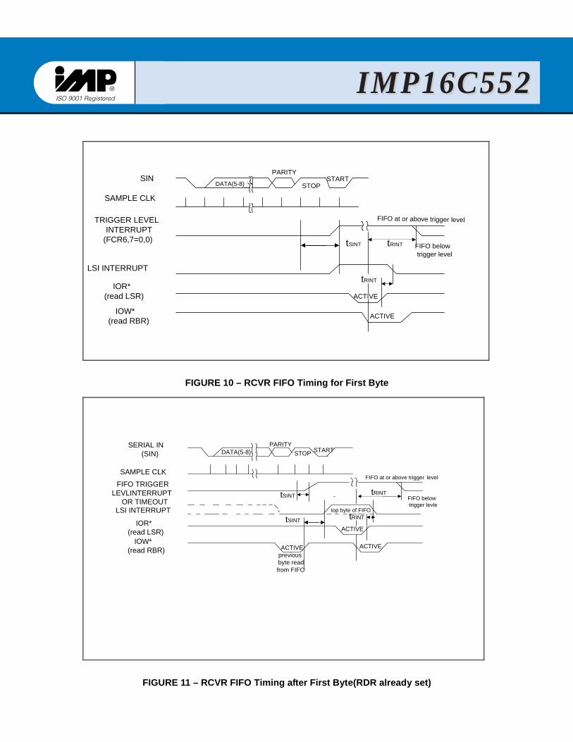
FIGURE 10 – RCVR FIFO Timing for First Byte
FIGURE 11 – RCVR FIFO Timing after First Byte(RDR already set)
ACTIVE
ACTIVE
tRINT
tSINT tRINT FIFO below trigger level
FIFO at or above trigger level
START STOP
PARITY
DATA(5-8) SIN
SAMPLE CLK
TRIGGER LEVEL INTERRUPT (FCR6,7=0,0)
LSI INTERRUPT
IOR* (read LSR)
IOW* (read RBR)
ACTIVE ACTIVE previous
byte read from FIFO
ACTIVE
tRINT
tRINT FIFO below
trigger levle
FIFO at or above trigger level
tSINT
tSINT
top byte of FIFO
STOP START PARITY SERIAL IN
(SIN)
SAMPLE CLK
FIFO TRIGGER LEVLINTERRUPT OR TIMEOUT LSI INTERRUPT
IOR* (read LSR)
IOW* (read RBR)
DATA(5-8)
29 408-432-9100/www.impweb.com © 2002 IMP, Inc.
IMP16C552IMP16C552

FIGURE 12 – Receiver DMA Timing (FCR0=0 or FCR0=1 and FCR3=0)
Mode 0
FIGURE 13 – Receiver DMA Timing (FCR0=1 and FCR3=1) Mode 1
tSINT tRINT
ACTIVE
Note1
STOP PARITY
IOR* (read RBR)
SIN0(first byte)
SAMPLE CLK
RXRDY*
Note 1 FCR0=1:Reading of last byte from FIFO FCR0=0:Reading RBR
tSINT
ACTIVE
Note1
STOP PARITY
tRINT
IOR* (read RBR)
SIN0(first byte that reaches
trigger level)
SAMPLE CLK
RXRDY*
Note 1 Reading of last byte from FIFO
30 408-432-9100/www.impweb.com © 2002 IMP, Inc.
IMP16C552IMP16C552

FIGURE 14 – Transmitter Timing
Symbol Parameter Min Max Units Test Conditions tHR tIR tIRS tSI tSTI tSXA tWXI
Delay from IOW* (WR THR) to Reset Interrupt Delay from IOR* (RD IIR) to Reset Interrupt(THRE) Delay from Initial INTRPT reset to transmit Start Delay from Initial Write to Interrupt Delay from Stop to Interrupt(THRE) Delay from Start to TXREY Active Delay from Write to TXRDY Inactive
0 16 8 0 0
50 250 12 32 8 8 60
nsec nsec BAUDOUT Cycles BAUDOUT Cycles BAUDOUT Cycles (note 1) BAUDOUT Cycles nsec
100pF Load 100pF Load (note 1) (note 1) 100pF Load 100pF Load
SERIAL OUT (SOUT)
THRE INTERRUPT
IOW*(1) (write THR)
IOR*(2) (read IIR)
NOTES: (1)See Write Cycle Timing (2)See Read Cycle Timing
START DATA(5-8) PARITY STOPtIRS
tHR
tSI
tHR
tSTI
START
tIR
31 408-432-9100/www.impweb.com © 2002 IMP, Inc.
IMP16C552IMP16C552
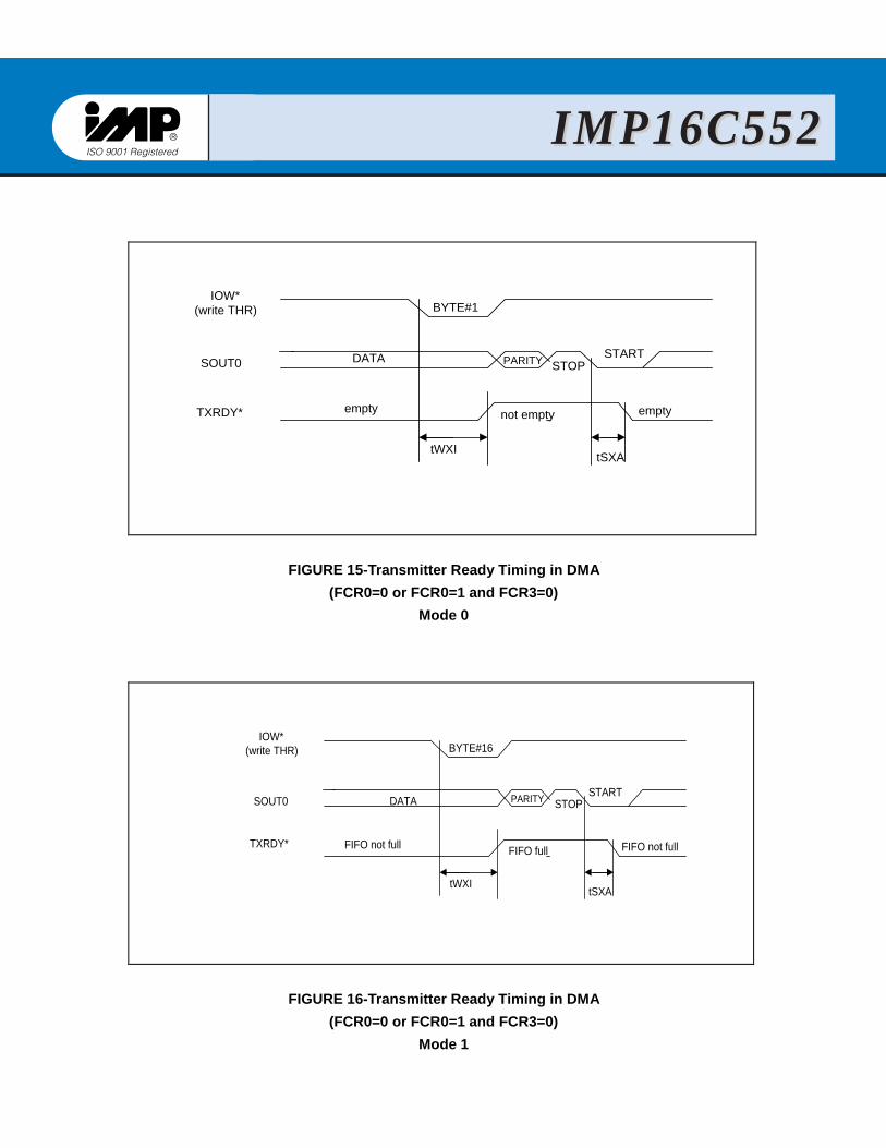
FIGURE 15-Transmitter Ready Timing in DMA
(FCR0=0 or FCR0=1 and FCR3=0) Mode 0
FIGURE 16-Transmitter Ready Timing in DMA
(FCR0=0 or FCR0=1 and FCR3=0) Mode 1
DATA
BYTE#16
PARITY STOP START
FIFO fullFIFO not full
tWXI tSXA
FIFO not full
IOW* (write THR)
SOUT0
TXRDY*
DATA
BYTE#1
PARITY STOP START
not empty empty
tWXI tSXA
empty
IOW* (write THR)
SOUT0
TXRDY*
32 408-432-9100/www.impweb.com © 2002 IMP, Inc.
IMP16C552IMP16C552

FIGURE 17- Parallel Port Timing
9
81716
2
3 4 10
7
5
Write Data
12 Read Data
1314
15 13
16
ADDRESS
11
CS2*
LPTOE*
A0,A1
D0-D7
IOW*
IOR*
PD0-PD7SLIN*,INIT*AFD*,STB*
IOW*
IOR*
D0-D7
ACK*
INT2
RESET*PD0-PD7
SLIN*,INIT*AFD*,STB*
33 408-432-9100/www.impweb.com © 2002 IMP, Inc.
IMP16C552IMP16C552

Symbol
Parameter Min Max Units Test Conditions
1 2 3 4 5 6 7 8 9 10 11 12 13 14 15 16 17
CS2* low to IOR*, IOW* low Address valid to IOR*, IOW* low Data setup to IOW* high Data hold to IOW* high IOW* high to PD0-PD7 IOW* high to INIT*, AFD*, SLIN*, STB* IOW*, IOR* high to CE* low Pulse width IOW* low Address hold after IOW*, IOR* high CS2* hold after IOW* IOR* high IOW* IOR* hold after CS2* high IOR* low to data valid IOR* high to D7-D0. Hi-Z ACK* to INT2 IOW* high to INT2 Hi-Z RST* low to D7-D0, SLIN*, STB* INIT*, AFD* LPTOE* low to PD0-PD7 Delay LPTOE* high to PD0-PD7Hi-Z
30 30 30 30 0 100 20 0 10
100 100 125 100 50 60 65 50 100
ns ns ns ns ns ns ns ns ns ns ns ns ns ns ns ns ns
ORDERING INFORMATION Part Number Package Operating Temperature IMP16C552-CJ68 68 pin PLCC 0�+70� IMP16C552-IJ68 68 pin PLCC -40�+85�
34 408-432-9100/www.impweb.com © 2002 IMP, Inc.
IMP16C552IMP16C552