


Idiomas
Páginas
Jurídico


Proyecto Fin de Carrera:
Placa solar con movimiento solidario al sol controlada mediante procesador
Antonio Jesús Merina Cárdenas 45736590-D
Proyecto Fin de carrera – Antonio Jesús Merina Cárdenas
Proyecto Fin de Carrera – Antonio Jesús Merina Cárdenas
ÍNDICE
PROYECTO FIN DE CARRERA: .................................................................. 1
PLACA SOLAR CON MOVIMIENTO SOLIDARIO AL SOL CONTROLADA MEDIANTE PROCESADOR ........................................................................ 1
1. INTRODUCCIÓN ............................................................................... 4
1.1 Una energía garantizada para los próximos 6.000 millones de años ................... 4 1.2 ¿Qué se puede hacer con la energía solar? .......................................................... 4 1.3 CALOR Y ELECTRICIDAD GARANTIZADOS ........................................................... 5 1.4 ¿En qué Beneficia La Energía Solar Al Medio Ambiente y a Mi Economía? ........ 6
1.4.1 Beneficios medioambientales ........................................................................ 6 1.4.2 Beneficios educativos .................................................................................... 6 1.4.3 Beneficios Económicos ................................................................................... 6 1.4.4 Beneficios Sociales ......................................................................................... 7 1.4.5 BOOM SOLAR.................................................................................................. 7 1.4.6 ¿Cómo aprovechar el sol? .............................................................................. 7 1.4.7 DÍAS SOLEADOS ............................................................................................. 8
1.5 ENERGÍA SOLAR TÉRMICA ................................................................................... 8 1.6 Diferentes Usos De la Energía Solar. .................................................................... 9
1.6.1 Colectores de Placas ...................................................................................... 9 1.6.2 Colectores de concentración .......................................................................... 9 1.6.3 Hornos solares ............................................................................................. 10 1.6.4 Electricidad fotovoltáica .............................................................................. 10 1.6.5 Dispositivos de almacenamiento de energía solar ....................................... 11
1.7 CÉLULAS FOTOVOLTAICAS ................................................................................. 11 1.7.1 ¿SOLOS O EN RED? ...................................................................................... 12
1.8 OPINIÓN PERSONAL .......................................................................................... 13
2. MOTIVACIÓN DEL PROYECTO ........................................................ 15
3. FOTODETECTORES ......................................................................... 16
4. CÁLCULO DE LA POSICIÓN DEL SOL .............................................. 18
5. COMPONENTES DEL PCB ................................................................ 20
5.1 Microcontrolador ................................................................................................ 20 5.2 Reguladores de tensión ...................................................................................... 21 5.3 Conjunto de INA´s: ............................................................................................ 23 5.4 Opamp ................................................................................................................ 23 5.5 Drivers de los motores ....................................................................................... 23
6. PCB RESULTANTE ........................................................................... 26
7. DISPOSITIVOS EXTERNOS AL CIRCUITO ....................................... 28
7.1 Placa fotovoltaica ............................................................................................... 29 7.2 Motores DC ......................................................................................................... 29 7.3 Batería 12 V ........................................................................................................ 29 7.4 Adaptador a placa PIC ........................................................................................ 30 7.5 Placa PIC (procesador) ....................................................................................... 31
8. POSIBLES MEJORAS AL PROYECTO ................................................ 31
8.1 Circuito de carga de la batería ........................................................................... 31 8.2 Array de células fotovoltaicas ............................................................................ 31
Proyecto Fin de carrera – Antonio Jesús Merina Cárdenas
Proyecto Fin de Carrera – Antonio Jesús Merina Cárdenas
8.3 Registro de Históricos y autoaprendizaje .......................................................... 32
9. RESULTADO FINAL ......................................................................... 32
10. ANEXOS: ...................................................................................... 37
Proyecto Fin de Carrera – Antonio Jesús Merina Cárdenas
Proyecto Fin de Carrera – Antonio Jesús Merina Cárdenas
1. INTRODUCCIÓN
1.1 Una energía garantizada para los próximos 6.000 millones de años El Sol, fuente de vida y origen de las demás formas de energía que el hombre ha utilizado desde los albores de la Historia, puede satisfacer todas nuestras necesidades, si aprendemos cómo aprovechar de forma racional la luz que continuamente derrama sobre el planeta. Ha brillado en el cielo desde hace unos cinco mil millones de años, y se calcula que todavía no ha llegado ni a la mitad de su existencia. Durante el presente año, el Sol arrojará sobre la Tierra cuatro mil veces más energía que la que vamos a consumir. España, por su privilegiada situación y climatología, se ve particularmente favorecida respecto al resto de los países de Europa, ya que sobre cada metro cuadrado de su suelo inciden al año unos 1.500 kilovatios-hora de energía, cifra similar a la de muchas regiones de América Central y del Sur. Esta energía puede aprovecharse directamente, o bien ser convertida en otras formas útiles como, por ejemplo, en electricidad. No sería racional no intentar aprovechar, por todos los medios técnicamente posibles, esta fuente energética gratuita, limpia e inagotable, que puede liberarnos definitivamente de la dependencia del petróleo o de otras alternativas poco seguras, contaminantes o, simplemente, agotables. Es preciso, no obstante, señalar que existen algunos problemas que debemos afrontar y superar. Aparte de las dificultades que una política energética solar avanzada conllevaría por sí misma, hay que tener en cuenta que esta energía está sometida a continuas fluctuaciones y a variaciones más o menos bruscas. Así, por ejemplo, la radiación solar es menor en invierno, precisamente cuando más la solemos necesitar. Es de vital importancia proseguir con el desarrollo de la incipiente tecnología de captación, acumulación y distribución de la energía solar, para conseguir las condiciones que la hagan definitivamente competitiva, a escala planetaria.
1.2 ¿Qué se puede hacer con la energía solar? Básicamente, recogiendo de forma adecuada la radiación solar, podemos obtener calor y electricidad. El calor se logra mediante los colectores térmicos, y la electricidad, a través de los llamados módulos fotovoltaicos. Ambos procesos nada tienen que ver entre sí, ni en cuanto a su tecnología ni en su aplicación. Hablemos primero de los sistemas de aprovechamiento térmico. El calor recogido en los colectores puede destinarse a satisfacer numerosas necesidades. Por ejemplo, se puede obtener agua caliente para consumo doméstico o industrial, o bien para dar calefacción a nuestros hogares, hoteles, colegios, fábricas, etc. Incluso podemos climatizar las piscinas y permitir el baño durante gran parte del año. También, y aunque pueda parecer extraño, otra de las más prometedoras aplicaciones del calor solar será la refrigeración durante las épocas cálidas .precisamente cuando más soleamiento hay. En efecto, para obtener frío hace falta disponer de un «foco cálido», el cual puede perfectamente tener su

Proyecto Fin de Carrera – Antonio Jesús Merina Cárdenas
Proyecto Fin de Carrera – Antonio Jesús Merina Cárdenas
origen en unos colectores solares instalados en el tejado o azotea. En los países árabes ya funcionan acondicionadores de aire que utilizan eficazmente la energía solar. Las aplicaciones agrícolas son muy amplias. Con invernaderos solares pueden obtenerse mayores y más tempranas cosechas; los secaderos agrícolas consumen mucha menos energía si se combinan con un sistema solar, y, por citar otro ejemplo, pueden funcionar plantas de purificación o desalinización de aguas sin consumir ningún tipo de combustible. Las «células solares», dispuestas en paneles solares, ya producían electricidad en los primeros satélites espaciales. Actualmente se perfilan como la solución definitiva al problema de la electrificación rural, con clara ventaja sobre otras alternativas, pues, al carecer los paneles de partes móviles, resultan totalmente inalterables al paso del tiempo, no contaminan ni producen ningún ruido en absoluto, no consumen combustible y no necesitan mantenimiento. Además, y aunque con menos rendimiento, funcionan también en días nublados, puesto que captan la luz que se filtra a través de las nubes. La electricidad que así se obtiene puede usarse de manera directa (por ejemplo para sacar agua de un pozo o para regar, mediante un motor eléctrico), o bien ser almacenada en acumuladores para usarse en las horas nocturnas. Incluso es posible inyectar la electricidad sobrante a la red general, obteniendo un importante beneficio. Si se consigue que el precio de las células solares siga disminuyendo, iniciándose su fabricación a gran escala, es muy probable que, para primeros de siglo, una buena parte de la electricidad consumida en los países ricos en sol tenga su origen en la conversión fotovoltaica. La energía solar puede ser perfectamente complementada con otras energías convencionales, para evitar la necesidad de grandes y costosos sistemas de acumulación. Así, una casa bien aislada puede disponer de agua caliente y calefacción solares, con el apoyo de un sistema convencional a gas o eléctrico que únicamente funcionaría en los periodos sin sol. El coste de la «factura de la luz» sería sólo una fracción del que alcanzaría sin la existencia de la instalación solar.
1.3 CALOR Y ELECTRICIDAD GARANTIZADOS El sol ofrece la posibilidad de generar calor y electricidad de una forma barata, respetuosa con el medio ambiente y proporcionando independencia energética. España es el país europeo que más radiación solar recibe junto a Portugal. Sin embargo, este potencial a penas se aprovecha ni por medio de la
Proyecto Fin de Carrera – Antonio Jesús Merina Cárdenas
Proyecto Fin de Carrera – Antonio Jesús Merina Cárdenas
energía solar térmica de baja temperatura ni por la solar fotovoltaica, que cuentan, de momento con una mínima implantación. La expresión "No hay nada nuevo bajo el Sol" deja patente la presencia que el rastro rey lleva ejerciendo desde antaño sobre la Tierra. No es para menos. Y es que se calcula que lleva emitiendo energía a nuestro planeta desde hace más de 4.000 millones de años. Durante todo este tiempo ha dejado constancia de su importancia por ser el motor que actúa directa o indirectamente en todas las manifestaciones de vida terrestre. Desde hace unos años, cada vez está cobrando más fuerza el papel que el Sol puede tener para evitar el deterioro del medio ambiente. ¿Cómo? Aprovechando la radiación solar que deja caer sobre la Tierra como fuente energética limpia, gratuita y autónoma. De esta forma, podría sustituir total o parcial-mente a las energías tradicionales -procedentes del petróleo, el gas, o el carbón, productoras de emisiones nocivas que dañan la salud humana y el entorno- y ofrecer, a cambio, una alternativa claramente beneficiosa. Por supuesto que el potencial que ofrecen los rayos solares no es nuevo. Pero hizo falta que la crisis del petróleo de la década de los setenta pusiera en entredicho la dependencia energética de nuestro país y la necesidad de buscar nuevas soluciones para conseguir autonomía en este sector. Este punto de inflexión vino acompañado de la reivindicación de distintos grupos sociales que solicitaron un cambio en la política energética para no dañar el entorno a través de las energías renovables.
1.4 ¿En qué Beneficia La Energía Solar Al Medio Ambiente y a Mi Economía? La energía solar, además de ser renovable y no contaminar el Medio Ambiente, es una energía muy abundante en España. Su utilización contribuye a reducir el efecto invernadero producido por las emisiones de CO2 a la atmósfera, así como el cambio climático provocado por el efecto invernadero. Además, con su difusión y promoción todos colaboramos a que en el futuro se aproveche también el Sol en otras escuelas y edificios.
1.4.1 Beneficios medioambientales Disminución de las emisiones de CO2. Por cada 20 kWh de electricidad producidos a partir de energía solar se dejan de emitir unos 10 Kg de CO2 al año, en 25 años se evitan 250 Kg de CO2. Reducción de la contaminación atmosférica, del efecto invernadero producido por las emisiones de CO2 y del cambio climático provocado por el efecto invernadero.
1.4.2 Beneficios educativos Educación de los alumnos en las tecnologías ecológicas y en la cultura de respeto al Medio Ambiente. Posibilidad de creación de un Club Solar en cada centro, que recoja, estudie y elabore trabajos sobre temas relacionados con la energía solar. Programación de actividades educativas relacionadas con la energía solar y la ecología: Semana Solar, concursos, exposiciones con los resultados de los trabajos, etc. Contacto e intercambio con otros centros incluidos en la Red de Escuelas Solares en España (y posiblemente en otros países).
1.4.3 Beneficios Económicos Cada kilovatio-hora (kWh) producido con energía solar fotovoltaica lo podemos cobrar a 66 Ptas (0.40 €). Una instalación de 5 kW de potencia puede producir al año entre 5.000 y 7.500 kWh, es decir, entre 330.000 ptas ( 1983.34 €) y 500.000 Ptas (3005.06 €) Una instalación de 5 kW de potencia cuesta aproximadamente unos 5 ó 6 millones ptas ( 30050.61 o 36060.73 €) y puede producir entre 150.000 y 187.500 kWh en 25-30 años, es decir, de 10 a 12 millones ptas ( 60101.21 € a 72121.45 €).
Proyecto Fin de Carrera – Antonio Jesús Merina Cárdenas
Proyecto Fin de Carrera – Antonio Jesús Merina Cárdenas
El beneficio total de la instalación solar es de 150.000 a 275.000 pts al año y entre 4,5 y 7 millones ( 27045.54 y 42070.85 €) a lo largo de los 25-30 años de funcionamiento. Con las ayudas de algunas entidades y administraciones públicas se puede conseguir hasta el 50% de la inversión. Este tipo de subvenciones a fondo perdido no han de devolverse posteriormente.
1.4.4 Beneficios Sociales Las energías renovables generan más puestos de trabajo que otras energías más contaminantes. Por cada 100 millones de pesetas invertidas en energía solar se crean entre 4 y 6 nuevos empleos. La misma inversión en energía procedente del petróleo sólo crearía 0,6 puestos de trabajo. Los puestos generados por la inversión en energía solar no son estacionarios (ligados a la construcción de una central, etc.), y se distribuyen a pequeña escala por todo el territorio. La utilización de energía solar en zonas rurales o aisladas, permite la creación de pequeñas empresas, lo que potencia el desarrollo económico de comarcas poco favorecidas.
1.4.5 BOOM SOLAR La década de los ochenta supuso el boom de la energía solar. Sin embargo, pronto se produjo un descenso de esta demanda motivado, según la mayoría de los expertos, por la decepción desencadenada, ya que muchas instalaciones duraron menos de lo previsto. La razón: falta de profesionalidad del sector al que sorprendió sin la suficiente cualificación, el auge de la energía solar. En estos momentos los compromisos del Protocolo de Kyoto de reducción de emisiones de gases de efecto invernadero conllevan no sólo un mayor uso eficiente de la energía sino también el impulso de las energías renovables. Con el objetivo de buscar estos mismos propósitos en 1999 España aprobó el Plan de Fomento de las Energías Renovables, que establece mecanismos no solo de eficiencia y ahorro de energía ara reducir el consumo energético sino también para conseguir que las energías renovables alcancen el 12 por ciento en la demanda de la energía primaria en el 2010. Esta cifra es una de las finalidades establecidas por el Libro Blanco de la Comisión Europea respecto al consumo de energías renovables. Si se consigue una mayor implantación, las energías renovables nos ofrecerán la ventaja de no hipotecar nuestro futuro medioambiental y continuar garantizando nuestro consumo.
1.4.6 ¿Cómo aprovechar el sol?
El rendimiento que el hombre puede hacer de la energía solar es variado. En este sentido, Jose Luis García, responsable de las campañas de energía de Greenpeace, señala que “dentro de la energía solar hay dos bloques: La energía solar pasiva y la activa. Se diferencian en que la pasiva aprovecha la energía sin la utilización de ningún sistema de conversión o transferencia de energía, la activa sí. Dentro de la energía solar activa, se incluiría la energía solar térmica, aquellos sistemas que aprovechan la energía del Sol para una demanda energética de calor y la energía solar fotovoltaica, aquella que convierte la luz del Sol en electricidad. Los mecanismos para obtener tanto el calor como la electricidad variarán tanto en la instalación requerida como en su aplicación. Así, en líneas generales hay que apuntar que el calor se logra por medio de los denominados colectores térmicos y la electricidad mediante los módulos fotovoltaicos. En un contexto de limitación de las energías convencionales, la radiación solar se desmarca con diferencia debido a que las grandes posibilidades productivas que emanan son muy superiores a la capacidad de consumo actual. De esta forma, según recoge el Centro de Estudios de la Energía Solar (CENSOLAR), "el Sol arrojará durante este año sobre la Tierra cuatro mil veces más de energía de la que vamos a consumir". Por su parte Greenpeace señala que "la cantidad que recibe la Tierra en 30
Proyecto Fin de Carrera – Antonio Jesús Merina Cárdenas
Proyecto Fin de Carrera – Antonio Jesús Merina Cárdenas
minutos es equivalen a toda la energía consumida por la humanidad en un año". Una radiación solar que seguirá llegando durante 6.000 años más.
1.4.7 DÍAS SOLEADOS
No todas las zonas del planeta reciben con misma intensidad los rayos solares. En nuestro país, donde la abundancia de días soleados se ha convertido en un reclamo turístico por excelencia, esta fuente de energía adquiere una importancia mayor que en otros lugares del mundo. Sobre esta situación afortunada han coincidido tanto diversas asociaciones conservacionistas, que defienden a ultranza el uso de la energía solar, como también organismo institucionales. Desde el Instituto para la Diversificación y Ahorro de la Energía (IDAE) se asegura que “España, gracias a su emplazamiento geográfico, dispone de una privilegiada radiación solar y cuenta, por tanto, con un enorme potencial para el aprovechamiento energético de este recurso que nos proporciona la Naturaleza”. Se estima que nuestro país recibe por cada metro cuadrado de su suelo unos 1500 kilovatios-hora de energía cada año. Un panorama inmejorable y sin embargo una presencia todavía mínima. El propio IDEA reconoce que en España “esta energía de tanta calidad aún no ha alcanzado el grado de implantación que se merece”. El interés para recurrir al uso de esta inagotable fuente energética en España no es nuevo, sino que procede de la década de los ochenta. Luis Iglesias, secretario general del IDEA, concretiza que “la energía solar en España está siendo tratada en nuestro país desde los años 1980-82 dentro de una política de ahorro y eficiencia. Fue en la década de los noventa cuando recibió un impulso mayor, ya que las energías renovables a finales de 1999 llegaron a suponer el 6 por ciento dentro del consumo total de energía". Dentro de este panorama, en cierta medida marginal, sobre el empleo de las energías renovables todavía es menor la contribución de baja temperatura y la fotovoltaica, y esta segunda está aún menos representada que la térmica.
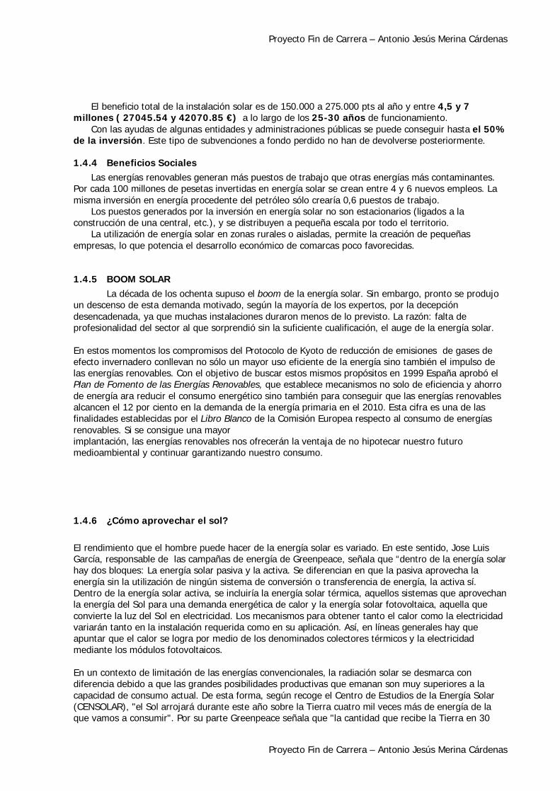
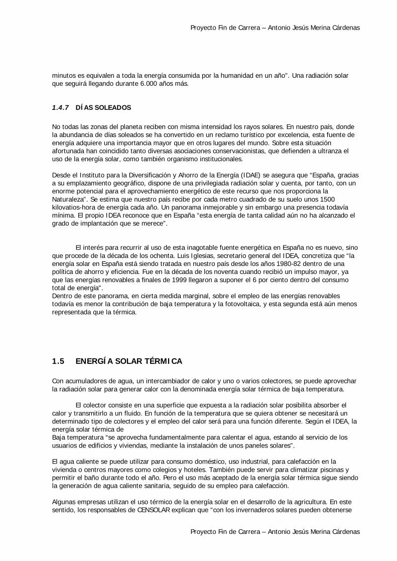
1.5 ENERGÍA SOLAR TÉRMICA Con acumuladores de agua, un intercambiador de calor y uno o varios colectores, se puede aprovechar la radiación solar para generar calor con la denominada energía solar térmica de baja temperatura. El colector consiste en una superficie que expuesta a la radiación solar posibilita absorber el calor y transmitirlo a un fluido. En función de la temperatura que se quiera obtener se necesitará un determinado tipo de colectores y el empleo del calor será para una función diferente. Según el IDEA, la energía solar térmica de Baja temperatura “se aprovecha fundamentalmente para calentar el agua, estando al servicio de los usuarios de edificios y viviendas, mediante la instalación de unos paneles solares”. El agua caliente se puede utilizar para consumo doméstico, uso industrial, para calefacción en la vivienda o centros mayores como colegios y hoteles. También puede servir para climatizar piscinas y permitir el baño durante todo el año. Pero el uso más aceptado de la energía solar térmica sigue siendo la generación de agua caliente sanitaria, seguido de su empleo para calefacción. Algunas empresas utilizan el uso térmico de la energía solar en el desarrollo de la agricultura. En este sentido, los responsables de CENSOLAR explican que “con los invernaderos solares pueden obtenerse
Proyecto Fin de Carrera – Antonio Jesús Merina Cárdenas
Proyecto Fin de Carrera – Antonio Jesús Merina Cárdenas
mayores y más tempranas cosechas”.Según se recomienda en la Guía Solar editada por Greenpeace:”con una instalación de 4m2 de captadores y 300 litros de acumulación de agua caliente se puede abastecer toda una familia (en función de la localidad, consumo, hábitos, etc.), ahorrando más de media tonelada de CO2 al año”. “Todo un interesante sistema de ahorro ya que una instalación térmica para generar agua caliente sanitaria puede sufragar el 70 por ciento de las necesidades de una casa”.
1.6 Diferentes Usos De la Energía Solar.
1.6.1 Colectores de Placas
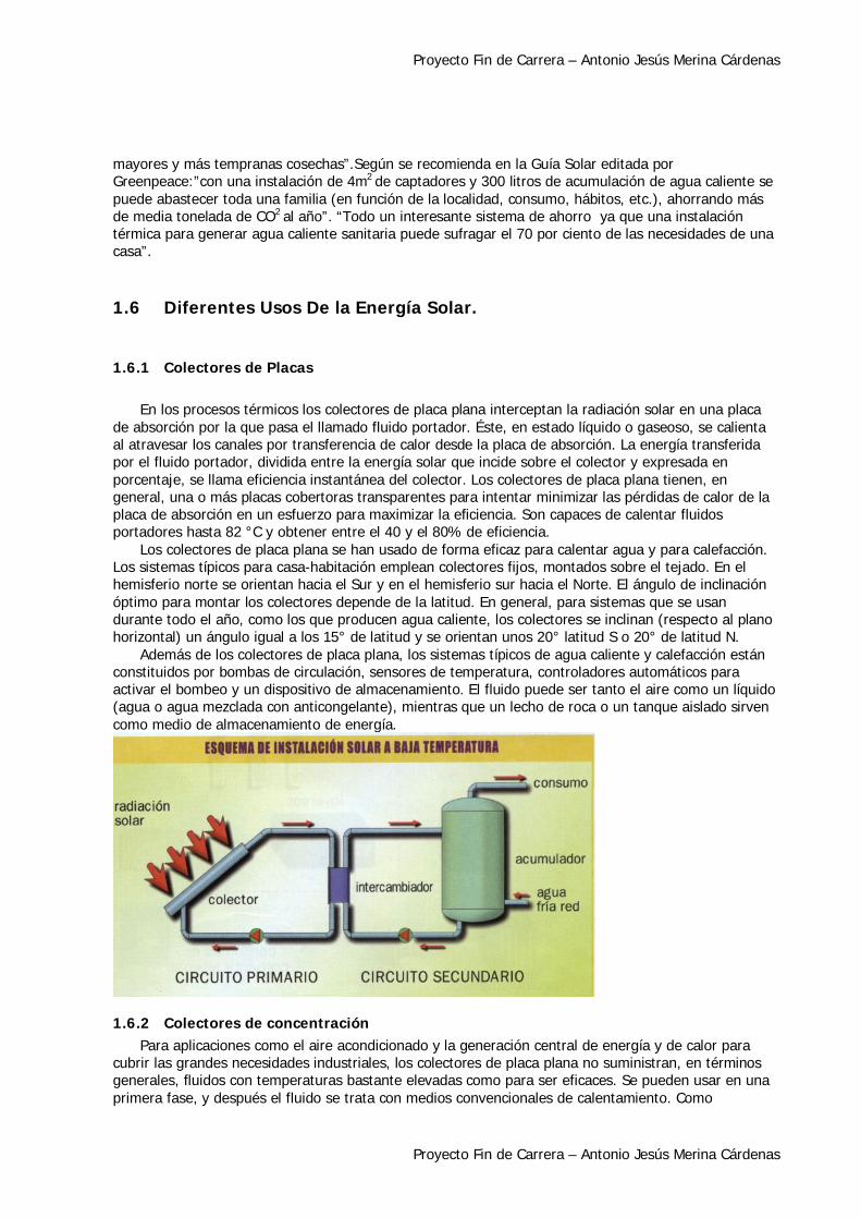
En los procesos térmicos los colectores de placa plana interceptan la radiación solar en una placa de absorción por la que pasa el llamado fluido portador. Éste, en estado líquido o gaseoso, se calienta al atravesar los canales por transferencia de calor desde la placa de absorción. La energía transferida por el fluido portador, dividida entre la energía solar que incide sobre el colector y expresada en porcentaje, se llama eficiencia instantánea del colector. Los colectores de placa plana tienen, en general, una o más placas cobertoras transparentes para intentar minimizar las pérdidas de calor de la placa de absorción en un esfuerzo para maximizar la eficiencia. Son capaces de calentar fluidos portadores hasta 82 °C y obtener entre el 40 y el 80% de eficiencia. Los colectores de placa plana se han usado de forma eficaz para calentar agua y para calefacción. Los sistemas típicos para casa-habitación emplean colectores fijos, montados sobre el tejado. En el hemisferio norte se orientan hacia el Sur y en el hemisferio sur hacia el Norte. El ángulo de inclinación óptimo para montar los colectores depende de la latitud. En general, para sistemas que se usan durante todo el año, como los que producen agua caliente, los colectores se inclinan (respecto al plano horizontal) un ángulo igual a los 15° de latitud y se orientan unos 20° latitud S o 20° de latitud N. Además de los colectores de placa plana, los sistemas típicos de agua caliente y calefacción están constituidos por bombas de circulación, sensores de temperatura, controladores automáticos para activar el bombeo y un dispositivo de almacenamiento. El fluido puede ser tanto el aire como un líquido (agua o agua mezclada con anticongelante), mientras que un lecho de roca o un tanque aislado sirven como medio de almacenamiento de energía.
1.6.2 Colectores de concentración Para aplicaciones como el aire acondicionado y la generación central de energía y de calor para cubrir las grandes necesidades industriales, los colectores de placa plana no suministran, en términos generales, fluidos con temperaturas bastante elevadas como para ser eficaces. Se pueden usar en una primera fase, y después el fluido se trata con medios convencionales de calentamiento. Como
Proyecto Fin de Carrera – Antonio Jesús Merina Cárdenas
Proyecto Fin de Carrera – Antonio Jesús Merina Cárdenas
alternativa, se pueden utilizar colectores de concentración más complejos y costosos. Son dispositivos que reflejan y concentran la energía solar incidente sobre una zona receptora pequeña. Como resultado de esta concentración, la intensidad de la energía solar se incrementa y las temperaturas del receptor (llamado ‘blanco’) pueden acercarse a varios cientos, o, de seguir al Sol vos utilizados para ello se llaman heliostatos.
1.6.3 Hornos solares Los hornos concentradores de alta temperatura. El mayor, situado en Odeillo, en la parte francesa de los Pirineos, tiene 9.600 reflectores con una superficie total de unos 1.900 m2 para producir temperaturas de hasta 4.000 °C. Estos hornos son ideales para investigaciones, por ejemplo, en la investigación de materiales, que requieren temperaturas altas en entornos libres de contaminantes.
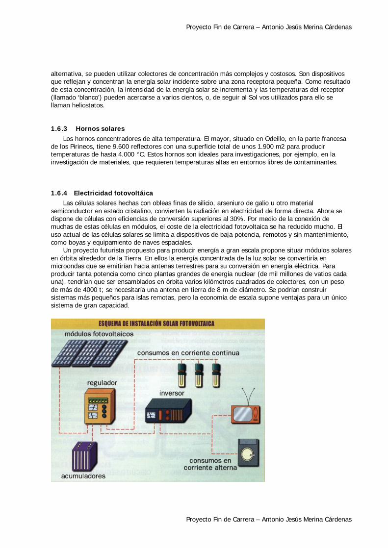
1.6.4 Electricidad fotovoltáica Las células solares hechas con obleas finas de silicio, arseniuro de galio u otro material semiconductor en estado cristalino, convierten la radiación en electricidad de forma directa. Ahora se dispone de células con eficiencias de conversión superiores al 30%. Por medio de la conexión de muchas de estas células en módulos, el coste de la electricidad fotovoltaica se ha reducido mucho. El uso actual de las células solares se limita a dispositivos de baja potencia, remotos y sin mantenimiento, como boyas y equipamiento de naves espaciales. Un proyecto futurista propuesto para producir energía a gran escala propone situar módulos solares en órbita alrededor de la Tierra. En ellos la energía concentrada de la luz solar se convertiría en microondas que se emitirían hacia antenas terrestres para su conversión en energía eléctrica. Para producir tanta potencia como cinco plantas grandes de energía nuclear (de mil millones de vatios cada una), tendrían que ser ensamblados en órbita varios kilómetros cuadrados de colectores, con un peso de más de 4000 t; se necesitaría una antena en tierra de 8 m de diámetro. Se podrían construir sistemas más pequeños para islas remotas, pero la economía de escala supone ventajas para un único sistema de gran capacidad.
Proyecto Fin de Carrera – Antonio Jesús Merina Cárdenas
Proyecto Fin de Carrera – Antonio Jesús Merina Cárdenas
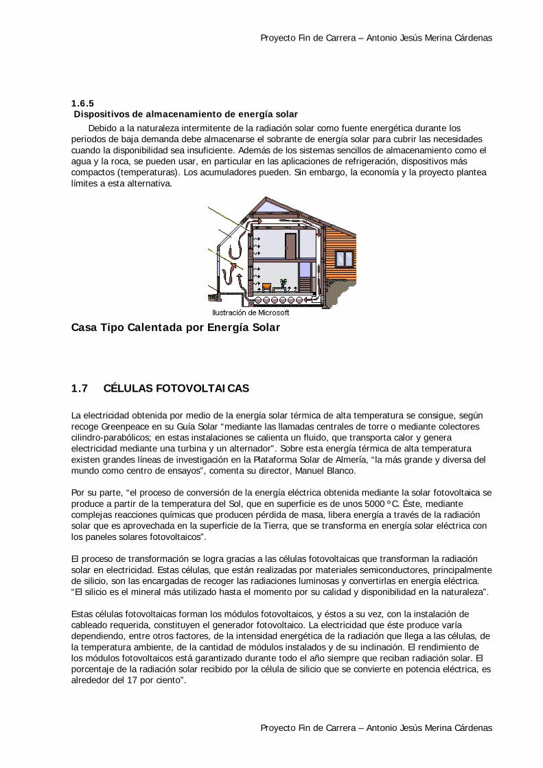
1.6.5 Dispositivos de almacenamiento de energía solar Debido a la naturaleza intermitente de la radiación solar como fuente energética durante los periodos de baja demanda debe almacenarse el sobrante de energía solar para cubrir las necesidades cuando la disponibilidad sea insuficiente. Además de los sistemas sencillos de almacenamiento como el agua y la roca, se pueden usar, en particular en las aplicaciones de refrigeración, dispositivos más compactos (temperaturas). Los acumuladores pueden. Sin embargo, la economía y la proyecto plantea límites a esta alternativa.
Casa Tipo Calentada por Energía Solar
1.7 CÉLULAS FOTOVOLTAICAS La electricidad obtenida por medio de la energía solar térmica de alta temperatura se consigue, según recoge Greenpeace en su Guía Solar “mediante las llamadas centrales de torre o mediante colectores cilindro-parabólicos; en estas instalaciones se calienta un fluido, que transporta calor y genera electricidad mediante una turbina y un alternador”. Sobre esta energía térmica de alta temperatura existen grandes líneas de investigación en la Plataforma Solar de Almería, “la más grande y diversa del mundo como centro de ensayos”, comenta su director, Manuel Blanco. Por su parte, “el proceso de conversión de la energía eléctrica obtenida mediante la solar fotovoltaica se produce a partir de la temperatura del Sol, que en superficie es de unos 5000 ºC. Éste, mediante complejas reacciones químicas que producen pérdida de masa, libera energía a través de la radiación solar que es aprovechada en la superficie de la Tierra, que se transforma en energía solar eléctrica con los paneles solares fotovoltaicos”. El proceso de transformación se logra gracias a las células fotovoltaicas que transforman la radiación solar en electricidad. Estas células, que están realizadas por materiales semiconductores, principalmente de silicio, son las encargadas de recoger las radiaciones luminosas y convertirlas en energía eléctrica. “El silicio es el mineral más utilizado hasta el momento por su calidad y disponibilidad en la naturaleza”. Estas células fotovoltaicas forman los módulos fotovoltaicos, y éstos a su vez, con la instalación de cableado requerida, constituyen el generador fotovoltaico. La electricidad que éste produce varía dependiendo, entre otros factores, de la intensidad energética de la radiación que llega a las células, de la temperatura ambiente, de la cantidad de módulos instalados y de su inclinación. El rendimiento de los módulos fotovoltaicos está garantizado durante todo el año siempre que reciban radiación solar. El porcentaje de la radiación solar recibido por la célula de silicio que se convierte en potencia eléctrica, es alrededor del 17 por ciento”.
Proyecto Fin de Carrera – Antonio Jesús Merina Cárdenas
Proyecto Fin de Carrera – Antonio Jesús Merina Cárdenas
Aunque son más productivos dependiendo de la época del año. En este sentido, Greenpeace señala que “normalmente en verano se genera más electricidad debido a la mayor duración del tiempo soleado. En los días nublados también se genera electricidad, aunque el rendimiento energético se reduce proporcionalmente por la menor intensidad de la radiación”. En la energía solar fotovoltaica lo importante es que la incidencia del rayo del Sol sea perpendicular a la placa y no necesita que el día sea especialmente caluroso como en el caso de la térmica. España es el primer productor europeo de placas fotovoltaicas de silicio cristalino y exporta la mayor parte de su producción a más de 50 países.
1.7.1 ¿SOLOS O EN RED?
La energía solar fotovoltaica tiene dos tipos de aplicaciones: los sistemas aislados y los conectados a la red. Los primeros son los que producen electricidad para autoabastecerse mientras que con los fotovoltaicos conectados a red cualquier usuario se convierte en productor y consumidor de su propia electricidad. En la elección de la instalación un sistema no es ni mejor ni peor que otro. Donde no hay red eléctrica el sistema autónomo es la mejor posibilidad, mientras que donde hay conexión a red no tiene sentido plantear el sistema aislado porque es más caro, siendo más lógica la otra opción”. EFICIENCIA ENERGÉTICA. Ahorrar energía es un camino eficaz e imprescindible para reducir las emisiones contaminantes de CO2 (dióxido de carbono) a la atmósfera, y por tanto detener el calentamiento global del planeta y el cambio climático. Es también el camino más sencillo y rápido para lograrlo. Por cada kilovatio-hora de electricidad que ahorremos, evitaremos la emisión de aproximadamente un kilogramo de CO2 en la central térmica donde se quema carbón o petróleo para producir esa electricidad. Además, ahorrar energía tiene otras ventajas adicionales para el medio ambiente, pues con ello evitamos: lluvias ácidas, mareas negras, contaminación del aire, residuos radiactivos, riesgo de accidentes nucleares, proliferación de armas atómicas, destrucción de bosques, devastación de parajes naturales, desertificación. Pero esas ventajas también alcanzan a nuestros bolsillos: cada kilovatio-hora le cuesta al consumidor 0,13 euros (en 2001), de forma que cambiar de hábitos o sustituir los aparatos por otros menos despilfarradores nos ahorra dinero; en algunos casos la alternativa que proponemos puede parecer más cara, pero lo que nos gastemos al principio lo recuperamos de manera más o menos rápida, pues habremos reducido el gasto en energía (factura de la luz, etc.) Una vez amortizado, comenzamos a ahorrar dinero (lo que dejamos de gastar en energía). Todas estas ventajas se traducen por sí mismas en una mejor calidad de vida, más aún si consumir menos energía va unido a la mejora de los servicios que ésta nos proporciona (luz, calor, movimiento...) es decir, se trata de mejorar la EFICIENCIA ENERGETICA. Así pondremos freno a la actual situación de despilfarro energético: en muchas ocasiones consumimos demasiada energía, que no necesitamos, recibiendo poco o ningún servicio y, a veces, un mal servicio e incluso perjuicios. Ahorrar energía es también un deber de solidaridad, si tenemos en cuenta que cada
Proyecto Fin de Carrera – Antonio Jesús Merina Cárdenas
Proyecto Fin de Carrera – Antonio Jesús Merina Cárdenas
habitante de los países desarrollados consume, por término medio, la misma energía que 16 ciudadanos del Tercer Mundo, y que los europeos occidentales somos responsables de la emisión de seis veces más cantidad de CO2 que los africanos.
1.8 OPINIÓN PERSONAL La aplicación de la energía solar en España choca con una serie de barreras o condicionantes que no han permitido hasta ahora alcanzar todo el desarrollo que debería haber tenido este tipo de energía en España. Los condicionantes que más influyen son los económicos financieros, falta de información y concienciación social hacia este tipo de tecnologías y la falta de cierta normativa específica. En edificación, y pese al avance que ha supuesto la aparición en el año 1998 del nuevo Reglamento de Instalaciones Térmicas en Edificios (RITE), en el que se introducen aplicaciones de la energía solar térmica, existen ciertas lagunas al respecto que hacen que la introducción de la energía solar en edificios no sea la deseada, siendo el resultado que los instaladores no prestan aún especial atención en la integración de la instalación solar en los edificios. En este contexto, y transcurrido un año desde la aprobación del Plan de Fomento de las Energías Renovables, el Gobierno, a través del IDAE, ha realizado actuaciones de apoyo e incentivación de la energía solar así como de impulso normativo. Las actuaciones de apoyo buscan un efecto multiplicador de las ayudas, así como fortalecer y consolidar una estructura sectorial de empresas instaladoras, con una calidad y durabilidad garantizadas de las instalaciones y alcanzar la concienciación ciudadana necesaria que permita su demanda hasta conseguir su utilización masiva. Así las líneas de apoyo puestas en marcha en el año 2000 fueron: Línea de apoyo a la energía solar Térmica de Baja Temperatura, destinada a la reducción del coste inicial de la instalación, a través de la modalidad de subvención directa a la inversión, mediante la formalización de una serie de convenios entre el IDAE y las empresas instaladoras acreditadas por el IDAE. Línea de financiación ICODAE para proyectos de inversión en ahorro y sustitución. Cogeneración y Energías Renovables, a través de la modalidad de préstamos con subvención al tipo de interés. Línea de Ayudas del IDAe para apoyo a la presentación de Propuestas al V programa Marco de I+D+D –programa energía- de la U.E. En el año 2001, además está previsto poner en marcha una línea de apoyo a la Energía Solar Fotovoltaica de potencia <100 kWe, destinada a la reducción del coste inicial de la instalación, a través de la modalidad de subvención directa a la inversión, mediante la formalización de una serie de convenios entre el IDAE y las empresas instaladoras acreditadas por el IDEA. El Real Decreto 1663/2000, de 29 de Septiembre, sobre conexión de instalaciones fotovoltacias a la red de baja tensión, por el que se establecen las condiciones técnicas y administrativas de la
Proyecto Fin de Carrera – Antonio Jesús Merina Cárdenas
Proyecto Fin de Carrera – Antonio Jesús Merina Cárdenas
conexión a red de baja tensión, facilitando y agilizando el trámite. También es importante mencionar el trabajo realizado por el Gobierno español en relación con la Directiva europea sobre la promoción de las energías renovables en el mercado interior de la electricidad, donde se defendió la posición española, que finalmente se tuvo en consideración en el borrador definitivo de la Directiva. La incentivación de la conexión a red de instalaciones fotovoltaicas, así como de su integración en edificios, no sólo se ha materializado a través de la publicación del Real Decreto, sino también a través de proyectos de demostración que permitan la maduración tecnológica industrial de la energía solar fotovoltaica. El IDAE realiza actuaciones de inversión-demostración, tendentes a dinamizar el mercado de las energías renovables e introducir las nuevas tecnologías. Por ello el gobierno, a raíz de la aprobación del Plan de Fomento de las Energías Renovables en España, sí está apostando por la energía solar y se están tomando las medidas necesarias que permitan que el aprovechamiento de esta fuente energética despegue en nuestro país. Hace 40 años, la industria aerospacial, en su programa Vanguard I aplicó los ensayos del laboratorio río Bell de N. Jersey (EE.UU) para lanzar al espacio células de silicio, capaces de aprovechar una fuente de energía procedente de las radiaciones solares y hacer funcionar el instrumental instalado a bordo. Hoy día su aplicación terrestre está muy extendida, especialmente en aquellas aplicaciones donde la energía convencional no llega fácilmente, y se está expandiendo como instrumento válido para evitar las emisiones de CO2 producidas por la combustión de materiales fósiles, en zonas que ya disfrutan de energía eléctrica. Las ventajas de la energía solar eléctrica son grandes frente a los inconvenientes superables. Podemos destacar como ventajas el aprovechamiento gratuito de las radiaciones solares, es una energía completamente renovable e inagotable, emplea materiales de larga duración (placas de silicio, mineral muy abundante en la naturaleza), se consume donde se produce, sin necesidad de grandes instalaciones concentradas, ayuda a la independencia energética. Además, las empresas españolas han desarrollado esta tecnología consiguiendo el primer lugar en la producción europea y el tercero en la producción mundial. Frente a estas ventajas, hay que superar los problemas de la financiación ocasionada por el desembolso inicial elevado y realizar proyectos con una adecuada integración en los edificios o lugares específicos. Su desarrollo masivo reducirá los precios y propiciará nuevas tecnologías para aumentar la eficiencia energética. El sector eléctrico tradicional español, actualmente tiene que afrontar varios retos históricos: liberalización del mercado, desarrollo de políticas de ahorro y eficiencia energética, diversificación de las fuentes para disminuir la dependencia exterior, respecto al medio ambiente, disminución de los precios de venta y todo ello garantizando la calidad del suministro, etc… En la energía solar encontramos una solución real para disponer de energía sin transportarla ni contaminar con emisiones perniciosas en su generación. España dispone de un nuevo sector ya consolidado en donde la investigación y el desarrollo de actividades de formación e información, significan, además de una valiosa aportación a la creación de empleo cualificado, una esperanza en el uso de nuevas tecnologías empleadas en beneficio de la humanidad. Con esta energía evitaremos riesgos excesivos ocasionados por otras fuentes de energía aparentemente más baratas.
Proyecto Fin de Carrera – Antonio Jesús Merina Cárdenas
Proyecto Fin de Carrera – Antonio Jesús Merina Cárdenas
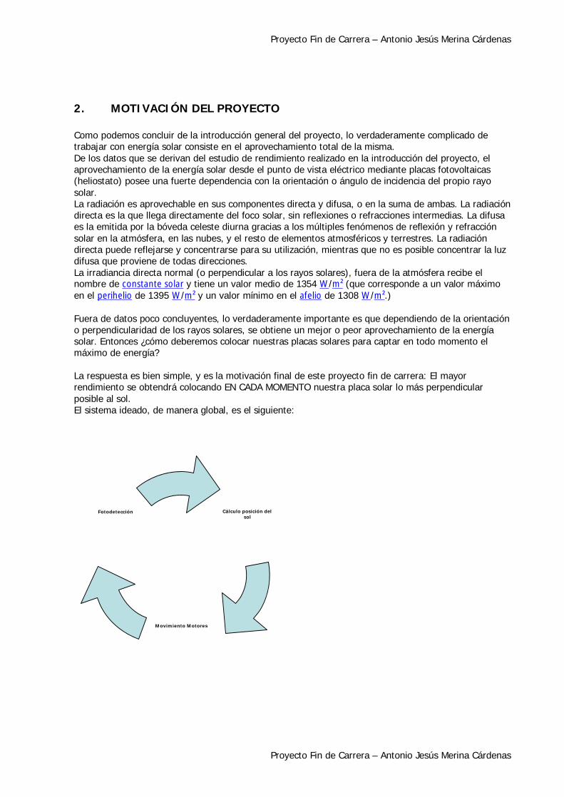
2. MOTIVACIÓN DEL PROYECTO Como podemos concluir de la introducción general del proyecto, lo verdaderamente complicado de trabajar con energía solar consiste en el aprovechamiento total de la misma. De los datos que se derivan del estudio de rendimiento realizado en la introducción del proyecto, el aprovechamiento de la energía solar desde el punto de vista eléctrico mediante placas fotovoltaicas (heliostato) posee una fuerte dependencia con la orientación o ángulo de incidencia del propio rayo solar. La radiación es aprovechable en sus componentes directa y difusa, o en la suma de ambas. La radiación directa es la que llega directamente del foco solar, sin reflexiones o refracciones intermedias. La difusa es la emitida por la bóveda celeste diurna gracias a los múltiples fenómenos de reflexión y refracción solar en la atmósfera, en las nubes, y el resto de elementos atmosféricos y terrestres. La radiación directa puede reflejarse y concentrarse para su utilización, mientras que no es posible concentrar la luz difusa que proviene de todas direcciones. La irradiancia directa normal (o perpendicular a los rayos solares), fuera de la atmósfera recibe el nombre de constante solar y tiene un valor medio de 1354 W/m² (que corresponde a un valor máximo en el perihelio de 1395 W/m² y un valor mínimo en el afelio de 1308 W/m².) Fuera de datos poco concluyentes, lo verdaderamente importante es que dependiendo de la orientación o perpendicularidad de los rayos solares, se obtiene un mejor o peor aprovechamiento de la energía solar. Entonces ¿cómo deberemos colocar nuestras placas solares para captar en todo momento el máximo de energía? La respuesta es bien simple, y es la motivación final de este proyecto fin de carrera: El mayor rendimiento se obtendrá colocando EN CADA MOMENTO nuestra placa solar lo más perpendicular posible al sol. El sistema ideado, de manera global, es el siguiente:
Cálculo posición del sol
Movimiento Motores
Fotodetección
Proyecto Fin de Carrera – Antonio Jesús Merina Cárdenas
Proyecto Fin de Carrera – Antonio Jesús Merina Cárdenas
3. FOTODETECTORES
La detección de radiación ultravioleta (UV) ha atraído una gran atención en los últimos años. Tanto la industria civil como la militar requieren una mejora en la instrumentación UV, para aplicaciones como control de motores, seguimiento de la radiación UV solar, calibración de emisores, estudios astronómicos, sensores de llama, detección de misiles, sistemas compactos de almacenamiento de información y comunicaciones espaciales seguras. Los nitruros del grupo III (GaN, AlN, InN y sus aleaciones ternarias) se han revelado como los materiales más prometedores para la fabricación de fotodetectores de UV basados en semiconductores, gracias a la anchura de su gap directo, que proporciona coeficientes de absorción elevados y una insensibilidad intrínseca a la radiación visible. Entre otras ventajas se incluyen la posibilidad de fabricar dispositivos de heterounión y de seleccionar la longitud de onda de corte modificando la fracción molar de los compuestos ternarios. Los fotoconductores son el dispositivo fotodetector más sencillo y económico, que consiste en dos contactos óhmicos depositados sobre una barra de material semiconductor. Se comportan como una resistencia cuyo valor óhmico depende de la intensidad luminosa incidente. Los fotoconductores de AlxGa1-xN presentan grandes responsividades a temperatura ambiente (100 para Popt = 1 W/m2), como resultado de una elevada ganancia interna. Desgraciadamente, esta ganancia está asociada a un comportamiento sublineal con la potencia óptica, un contraste UV/visible reducido y efectos persistentes. Estos inconvenientes hacen que los fotoconductores resulten inadecuados para la mayor parte de las aplicaciones. Tanto la linealidad como el rechazo al visible mejoran significativamente mediante un sistema de detección síncrono, utilizando un amplificador lock-in. Sin embargo, en esta configuración los fotoconductores pierden todas sus ventajas, ya que la responsividad disminuye y el sistema de medida se complica y encarece. Se ha desarrollado un modelo teórico que explica el comportamiento de estos dispositivos, tanto en lo referente a ganancia como a tiempos de respuesta, basándose en las zonas de carga espacial asociadas a las dislocaciones e intercaras. Este modelo presenta validez general, permitiendo justificar comportamientos no lineales observados en distintos materiales semiconductores. También se han fabricado fotodiodos Schottky planares, con contactos Schottky semitransparentes de distintos metales. Estos dispositivos presentan una responsividad aproximadamente constante para excitación con radiación de energía superior al gap del semiconductor, independientemente de la potencia óptica y de la temperatura. Su respuesta espectral muestra un corte abrupto, con un contraste UV/visible de 103. El tiempo de respuesta de estos dispositivos está limitado por su producto RC, con constantes de tiempo mínimas en el rango de nanosegundos. Se ha efectuado un análisis teórico de la respuesta de estos dispositivos, concluyéndose que su responsividad está todavía limitada por la elevada densidad de dislocaciones existentes en este material. De hecho, se ha verificado que los fotodiodos fabricados sobre GaN recrecido lateralmente (con una densidad de dislocaciones dos órdenes de magnitud inferior que el GaN típico) presentan un rechazo al visible un orden de magnitud superior, mayor ancho de banda y mayor detectividad. Se ha demostrado que los fotodiodos Schottky son adecuados para aplicaciones medioambientales, como la evaluación de la radiación UV solar, o para transmisión de datos a baja velocidad (MHz). Por otra parte, se han fabricado fotodiodos metal-semiconductor-metal (MSM) consistentes en dos contactos Schottky interdigitados sobre capas semi-aislantes de AlxGa1-xN. Estos dispositivos presentan muy bajas corrientes en oscuridad, se comportan linealmente con la potencia óptica y su contraste UV/visible supera 104. Su estructura planar permite conseguir un gran ancho de banda (en el rango de los GHz), que, con sus bajos niveles de ruido, hace que estos detectores sean los mejores candidatos para la fabricación receptores en comunicaciones ópticas en el rango UV. Desde el punto de vista de esta aplicación, resulta de especial interés el rango de longitudes de onda >280 nm, para comunicaciones entre satélites, que no podrían interferirse desde la Tierra gracias a la presencia del ozono estratosférico. Para trabajar en este rango son necesarios contenidos de Al superiores al 30%, donde es muy difícil depositar contactos óhmicos de calidad razonable. Los fotodiodos MSM, que
Proyecto Fin de Carrera – Antonio Jesús Merina Cárdenas
Proyecto Fin de Carrera – Antonio Jesús Merina Cárdenas
no precisan de contactos óhmicos, constituyen una prometedora alternativa tecnológica. Además, una ventaja añadida de estos dispositivos es su facilidad de integración con transistores de efecto campo. Los fotodiodos de unión p-n y p-i-n basados en AlxGa1-xN son lineales con la potencia óptica y presentan un contraste UV/visible de 104. Sin embargo, su tiempo de respuesta suele estar limitado por el comportamiento de los centros relacionados con el dopante tipo p (Mg), que también pueden deteriorar la respuesta espectral. Por otra parte, la longitud de onda de corte mínima que puede alcanzarse con estos dispositivos está limitada por la dificultad de conseguir conducción tipo p en AlxGa1-xN con contenidos de Al superiores al 15%. Aunque los resultados son prometedores, resulta todavía necesario un esfuerzo investigador en el dopaje tipo p del AlxGa1-xN para mejorar las prestaciones de estos detectores. En conclusión, los resultados actuales confirman a las aleaciones de AlxGa1-xN como los semiconductores más adecuados para la fotodetección en el rango ultravioleta del espectro. A partir de capas epitaxiales de semiconductor se ha desarrollado la tecnología de fabricación de distintos modelos de fotodetectores, con resultados competitivos a nivel comercial. Se han obtenido dispositivos con bajas corrientes de oscuridad, velocidad de respuesta en el rango de los picosegundos y detectividades >1011 cmW-1Hz1/2, comparables a los fotodiodos comerciales de silicio. Además, la insensibilidad de estos materiales a las radiaciones visible e infrarroja abre el camino a un nuevo tipo de sensores que pueden operar en presencia de fondos calientes, evitando el coste adicional y los efectos de envejecimiento debidos a los filtros. Como prueba de estos resultados, la Tesis se completa con la demostración de un prototipo de sistema automatizado para medida de la radiación solar UV.
Proyecto Fin de Carrera – Antonio Jesús Merina Cárdenas
Proyecto Fin de Carrera – Antonio Jesús Merina Cárdenas
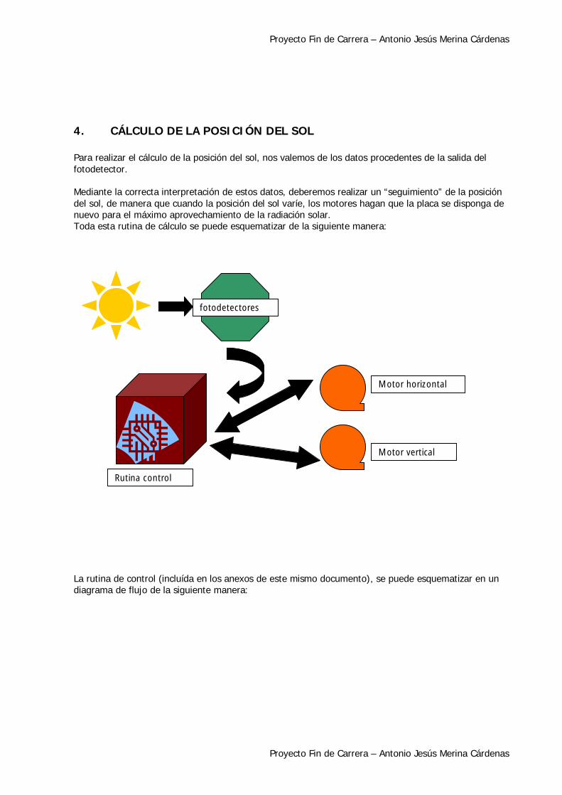
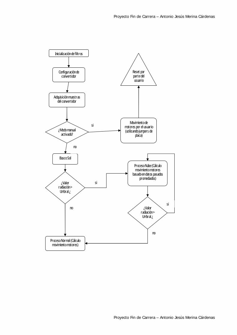
4. CÁLCULO DE LA POSICIÓN DEL SOL Para realizar el cálculo de la posición del sol, nos valemos de los datos procedentes de la salida del fotodetector. Mediante la correcta interpretación de estos datos, deberemos realizar un “seguimiento” de la posición del sol, de manera que cuando la posición del sol varíe, los motores hagan que la placa se disponga de nuevo para el máximo aprovechamiento de la radiación solar. Toda esta rutina de cálculo se puede esquematizar de la siguiente manera:
La rutina de control (incluída en los anexos de este mismo documento), se puede esquematizar en un diagrama de flujo de la siguiente manera:
fotodetectores
Motor horizontal
Motor vertical
Rutina control
Proyecto Fin de Carrera – Antonio Jesús Merina Cárdenas
Proyecto Fin de Carrera – Antonio Jesús Merina Cárdenas
Inicialización de filtros
Configuración de convertidor
Adquisición muestras del convertidor
Busco Sol
Proceso Normal (Cálculo movimiento motores)
Proceso Nube (Cálculo movimiento motores
basado en datos pasados promediados)
¿Valor radiación >
Umbral ¿
no
si
si
no
¿Modo manual activado?
¿Valor radiación >
Umbral ¿
si
no
Movimiento de motores por el usuario (utilizando jumpers de
placa)
Reset por parte del usuario

Proyecto Fin de Carrera – Antonio Jesús Merina Cárdenas
Proyecto Fin de Carrera – Antonio Jesús Merina Cárdenas
5. COMPONENTES DEL PCB En este apartado describiremos de una manera global lo diferentes módulos de los que se compone la placa o pcb. El “datasheet” de cada componente se encuentra en la sección “anexos” de este mismo documento. Podemos distinguir dentro de la placa los siguientes módulos:
1.- Microcontrolador 2.- Convertidores / Reguladores de tensión 3.- Conjunto de INA´s 4.- Opamp 5.- Drivers de los motores
5.1 Microcontrolador En un principio el sistema constaba de un Microcontrolador Motorola MMC2107 sobre placa PCB. Ver en anexo características de catálogo del Micro). Dicho microcontrolador realizaría la lógica de control de los motores gracias a los datos recogidos de los fotodetectores (y procesados por los filtros y el convertidor). Mediante sus puertos de salida, controlaría los leds de diagnostico, las señales de entrada de los drivers de los motores y recogería los datos del convertidor. El código residente en él (mientras se pretendía utilizar) se encuentra en la sección de anexos de este documento.
Proyecto Fin de Carrera – Antonio Jesús Merina Cárdenas
Proyecto Fin de Carrera – Antonio Jesús Merina Cárdenas
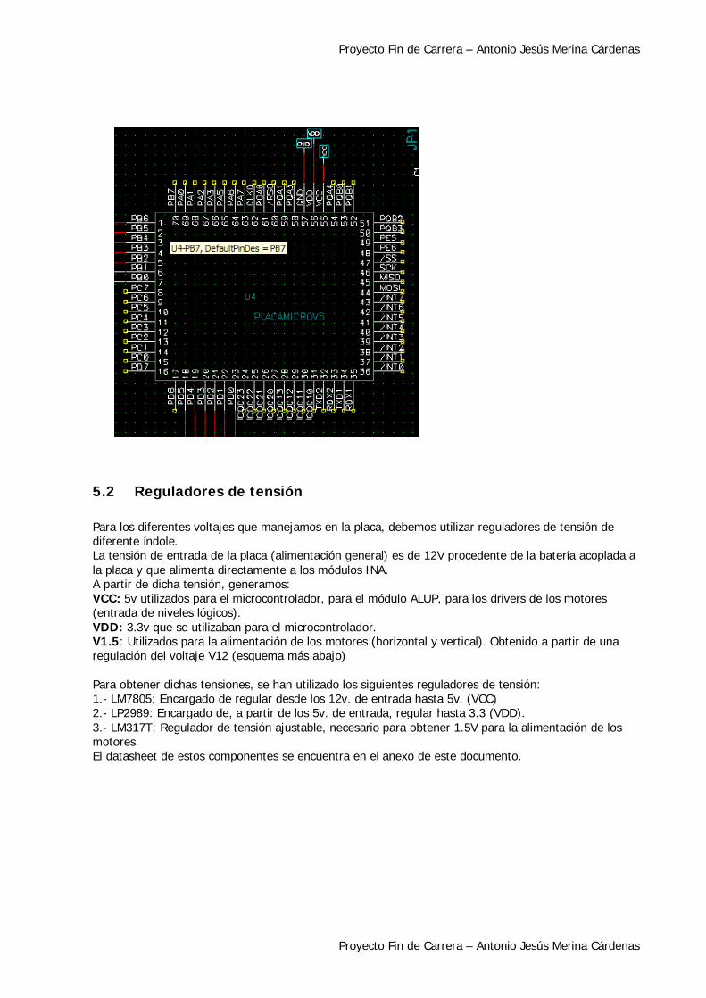
5.2 Reguladores de tensión
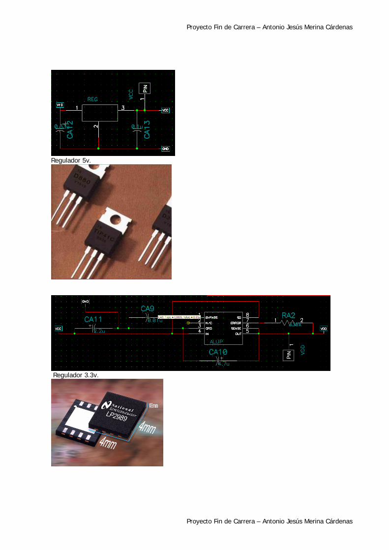
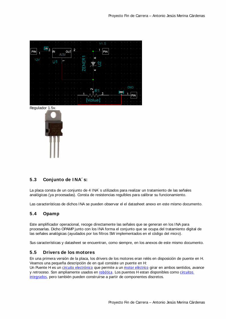
Para los diferentes voltajes que manejamos en la placa, debemos utilizar reguladores de tensión de diferente índole. La tensión de entrada de la placa (alimentación general) es de 12V procedente de la batería acoplada a la placa y que alimenta directamente a los módulos INA. A partir de dicha tensión, generamos: VCC: 5v utilizados para el microcontrolador, para el módulo ALUP, para los drivers de los motores (entrada de niveles lógicos). VDD: 3.3v que se utilizaban para el microcontrolador. V1.5: Utilizados para la alimentación de los motores (horizontal y vertical). Obtenido a partir de una regulación del voltaje V12 (esquema más abajo) Para obtener dichas tensiones, se han utilizado los siguientes reguladores de tensión: 1.- LM7805: Encargado de regular desde los 12v. de entrada hasta 5v. (VCC) 2.- LP2989: Encargado de, a partir de los 5v. de entrada, regular hasta 3.3 (VDD). 3.- LM317T: Regulador de tensión ajustable, necesario para obtener 1.5V para la alimentación de los motores. El datasheet de estos componentes se encuentra en el anexo de este documento.
Proyecto Fin de Carrera – Antonio Jesús Merina Cárdenas
Proyecto Fin de Carrera – Antonio Jesús Merina Cárdenas
Regulador 5v.
Regulador 3.3v.
Proyecto Fin de Carrera – Antonio Jesús Merina Cárdenas
Proyecto Fin de Carrera – Antonio Jesús Merina Cárdenas
Regulador 1.5v.
5.3 Conjunto de INA´s: La placa consta de un conjunto de 4 INA´s utilizados para realizar un tratamiento de las señales analógicas (ya procesadas). Consta de resistencias regulbles para calibrar su funcionamiento. Las características de dichos INA se pueden observar el el datasheet anexo en este mismo documento.
5.4 Opamp Este amplificador operacional, recoge directamente las señales que se generan en los INA para procesarlas. Dicho OPAMP junto con los INA forma el conjunto que se ocupa del tratamiento digital de las señales analógicas (ayudados por los filtros SW implementados en el código del micro). Sus características y datasheet se encuentran, como siempre, en los anexos de este mismo documento.
5.5 Drivers de los motores En una primera versión de la placa, los drivers de los motores eran relés en disposición de puente en H. Veamos una pequeña descripción de en qué consiste un puente en H: Un Puente H es un circuito electrónico que permite a un motor eléctrico girar en ambos sentidos, avance y retroceso. Son ampliamente usados en robótica. Los puentes H estan disponibles como circuitos integrados, pero también pueden construirse a partir de componentes discretos.
Proyecto Fin de Carrera – Antonio Jesús Merina Cárdenas
Proyecto Fin de Carrera – Antonio Jesús Merina Cárdenas
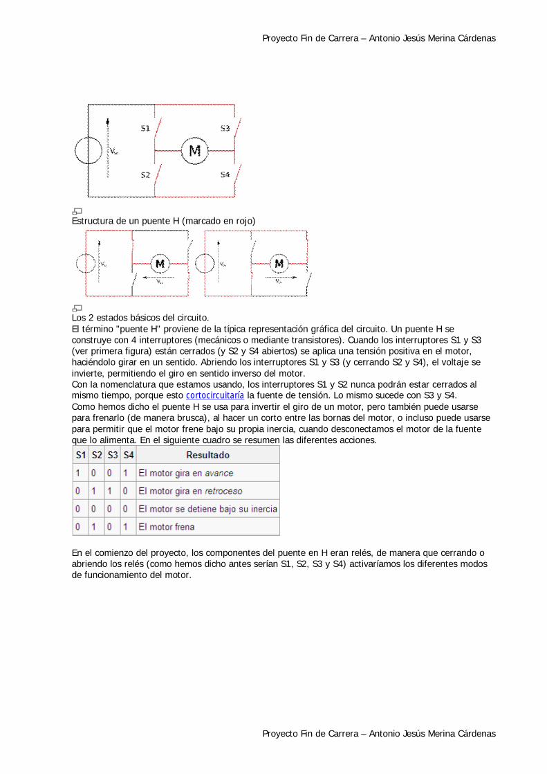
Estructura de un puente H (marcado en rojo)
Los 2 estados básicos del circuito. El término "puente H" proviene de la típica representación gráfica del circuito. Un puente H se construye con 4 interruptores (mecánicos o mediante transistores). Cuando los interruptores S1 y S3 (ver primera figura) están cerrados (y S2 y S4 abiertos) se aplica una tensión positiva en el motor, haciéndolo girar en un sentido. Abriendo los interruptores S1 y S3 (y cerrando S2 y S4), el voltaje se invierte, permitiendo el giro en sentido inverso del motor. Con la nomenclatura que estamos usando, los interruptores S1 y S2 nunca podrán estar cerrados al mismo tiempo, porque esto cortocircuitaría la fuente de tensión. Lo mismo sucede con S3 y S4. Como hemos dicho el puente H se usa para invertir el giro de un motor, pero también puede usarse para frenarlo (de manera brusca), al hacer un corto entre las bornas del motor, o incluso puede usarse para permitir que el motor frene bajo su propia inercia, cuando desconectamos el motor de la fuente que lo alimenta. En el siguiente cuadro se resumen las diferentes acciones.
En el comienzo del proyecto, los componentes del puente en H eran relés, de manera que cerrando o abriendo los relés (como hemos dicho antes serían S1, S2, S3 y S4) activaríamos los diferentes modos de funcionamiento del motor.
Proyecto Fin de Carrera – Antonio Jesús Merina Cárdenas
Proyecto Fin de Carrera – Antonio Jesús Merina Cárdenas
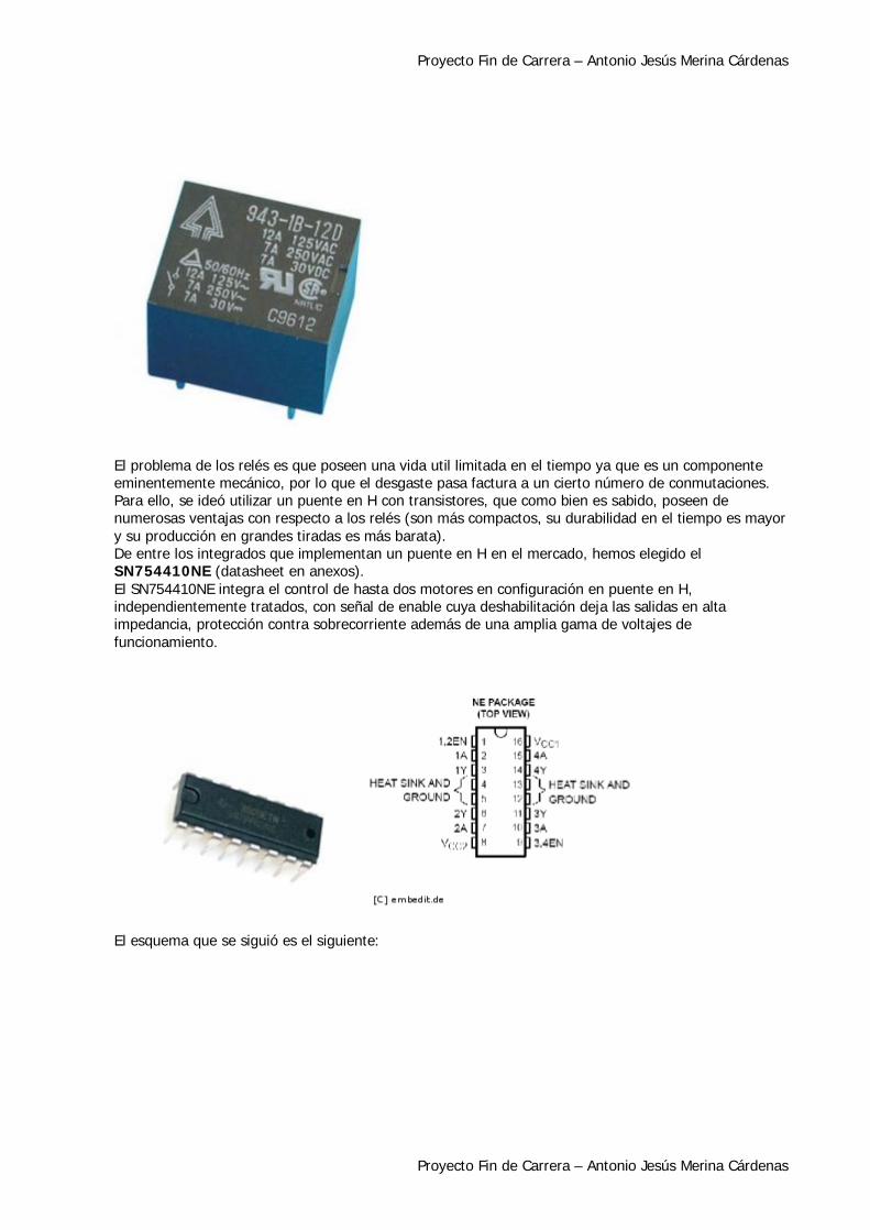
El problema de los relés es que poseen una vida util limitada en el tiempo ya que es un componente eminentemente mecánico, por lo que el desgaste pasa factura a un cierto número de conmutaciones. Para ello, se ideó utilizar un puente en H con transistores, que como bien es sabido, poseen de numerosas ventajas con respecto a los relés (son más compactos, su durabilidad en el tiempo es mayor y su producción en grandes tiradas es más barata). De entre los integrados que implementan un puente en H en el mercado, hemos elegido el SN754410NE (datasheet en anexos). El SN754410NE integra el control de hasta dos motores en configuración en puente en H, independientemente tratados, con señal de enable cuya deshabilitación deja las salidas en alta impedancia, protección contra sobrecorriente además de una amplia gama de voltajes de funcionamiento.
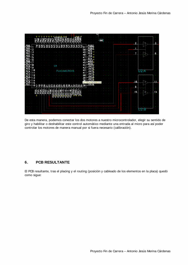
El esquema que se siguió es el siguiente:
Proyecto Fin de Carrera – Antonio Jesús Merina Cárdenas
Proyecto Fin de Carrera – Antonio Jesús Merina Cárdenas
De esta manera, podemos conectar los dos motores a nuestro microcontrolador, elegir su sentido de giro y habilitar o deshabilitar este control automático mediante una entrada al micro para así poder controlar los motores de manera manual por si fuera necesario (calibración).
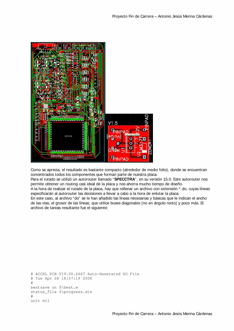
6. PCB RESULTANTE El PCB resultante, tras el placing y el routing (posición y cableado de los elementos en la placa) quedó como sigue:
Proyecto Fin de Carrera – Antonio Jesús Merina Cárdenas
Proyecto Fin de Carrera – Antonio Jesús Merina Cárdenas
Como se aprecia, el resultado es bastante compacto (alrededor de medio folio), donde se encuentran concentrados todos los componentes que forman parte de nuestra placa. Para el rutado se utilizó un autorouter llamado “SPECCTRA”, en su versión 15.0. Este autorouter nos permite obtener un routing casi ideal de la placa y nos ahorra mucho tiempo de diseño. A la hora de realizar el rutado de la placa, hay que rellenar un archivo con extensión *.do, cuyas líneas especificarán al autorouter las decisiones a llevar a cabo a la hora de enlutar la placa. En este caso, al archivo “do” se le han añadido las líneas necesarias y básicas que le indican el ancho de las vías, el grosor de las líneas, que utilice buses diagonales (no en ángulo recto) y poco más. El archivo de tareas resultante fue el siguiente: # ACCEL PCB V19.00.6667 Auto-Generated DO File # Tue Apr 08 18:57:19 2008 # bestsave on $\best.w status_file $\progress.sts # unit mil
Proyecto Fin de Carrera – Antonio Jesús Merina Cárdenas
Proyecto Fin de Carrera – Antonio Jesús Merina Cárdenas
# grid wire 100.000000 grid via 100.000000 merina bus diagonal # rule pcb (width 29) # bus diagonal route 50 clean 4 route 50 16 clean 4 filter 5 route 100 16 clean 2 delete conflicts # write wire $\placamerina10PCB.w spread miter write wire $\placamerina10PCB.m # write session $\placamerina10PCB.ses report status $\placamerina10PCB.sts
7. DISPOSITIVOS EXTERNOS AL CIRCUITO Como dispositivos externos al circuito tenemos:
1. Placa fotovoltaica 2. Motores DC 3. Batería 12V 4. Adaptador a placa PIC 5. Placa PIC (procesador)
Proyecto Fin de Carrera – Antonio Jesús Merina Cárdenas
Proyecto Fin de Carrera – Antonio Jesús Merina Cárdenas
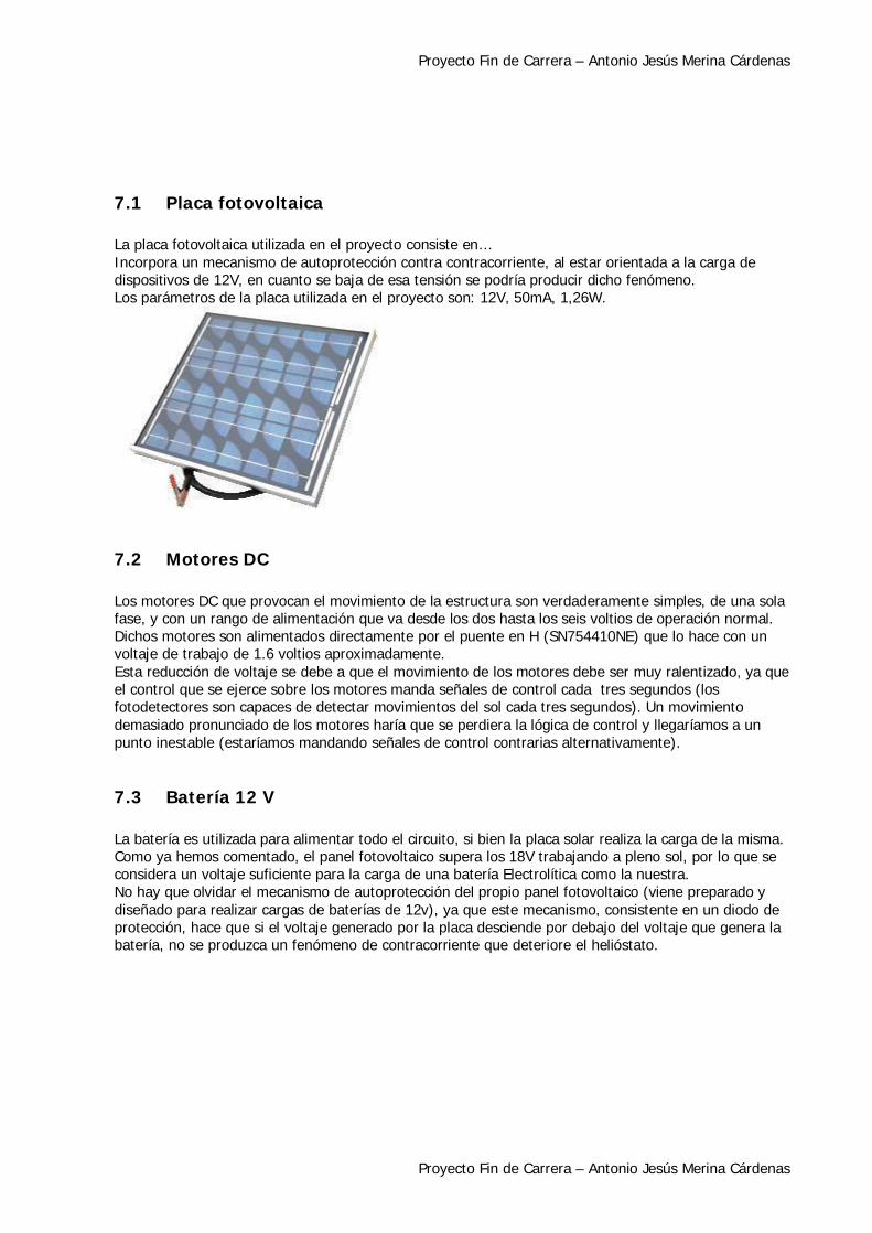
7.1 Placa fotovoltaica La placa fotovoltaica utilizada en el proyecto consiste en… Incorpora un mecanismo de autoprotección contra contracorriente, al estar orientada a la carga de dispositivos de 12V, en cuanto se baja de esa tensión se podría producir dicho fenómeno. Los parámetros de la placa utilizada en el proyecto son: 12V, 50mA, 1,26W.
7.2 Motores DC Los motores DC que provocan el movimiento de la estructura son verdaderamente simples, de una sola fase, y con un rango de alimentación que va desde los dos hasta los seis voltios de operación normal. Dichos motores son alimentados directamente por el puente en H (SN754410NE) que lo hace con un voltaje de trabajo de 1.6 voltios aproximadamente. Esta reducción de voltaje se debe a que el movimiento de los motores debe ser muy ralentizado, ya que el control que se ejerce sobre los motores manda señales de control cada tres segundos (los fotodetectores son capaces de detectar movimientos del sol cada tres segundos). Un movimiento demasiado pronunciado de los motores haría que se perdiera la lógica de control y llegaríamos a un punto inestable (estaríamos mandando señales de control contrarias alternativamente).
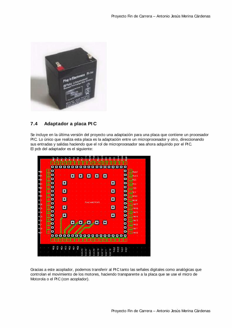
7.3 Batería 12 V La batería es utilizada para alimentar todo el circuito, si bien la placa solar realiza la carga de la misma. Como ya hemos comentado, el panel fotovoltaico supera los 18V trabajando a pleno sol, por lo que se considera un voltaje suficiente para la carga de una batería Electrolítica como la nuestra. No hay que olvidar el mecanismo de autoprotección del propio panel fotovoltaico (viene preparado y diseñado para realizar cargas de baterías de 12v), ya que este mecanismo, consistente en un diodo de protección, hace que si el voltaje generado por la placa desciende por debajo del voltaje que genera la batería, no se produzca un fenómeno de contracorriente que deteriore el helióstato.
Proyecto Fin de Carrera – Antonio Jesús Merina Cárdenas
Proyecto Fin de Carrera – Antonio Jesús Merina Cárdenas
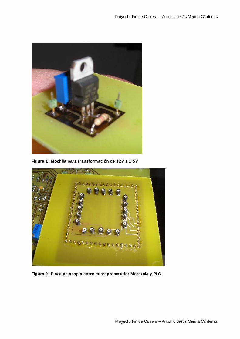
7.4 Adaptador a placa PIC Se incluye en la última versión del proyecto una adaptación para una placa que contiene un procesador PIC. Lo único que realiza esta placa es la adaptación entre un microprocesador y otro, direccionando sus entradas y salidas haciendo que el rol de microprocesador sea ahora adquirido por el PIC. El pcb del adaptador es el siguiente:
Gracias a este acoplador, podemos transferir al PIC tanto las señales digitales como analógicas que controlan el movimiento de los motores, haciendo transparente a la placa que se use el micro de Motorola o el PIC (con acoplador).
Proyecto Fin de Carrera – Antonio Jesús Merina Cárdenas
Proyecto Fin de Carrera – Antonio Jesús Merina Cárdenas
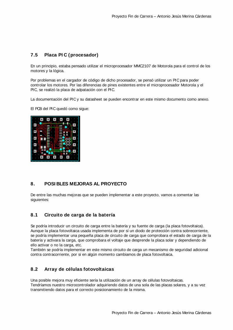
7.5 Placa PIC (procesador) En un principio, estaba pensado utilizar el microprocesador MMC2107 de Motorola para el control de los motores y la lógica. Por problemas en el cargador de código de dicho procesador, se pensó utilizar un PIC para poder controlar los motores. Por las diferencias de pines existentes entre el microprocesador Motorola y el PIC, se realizó la placa de adpatación con el PIC. La documentación del PIC y su datasheet se pueden encontrar en este mismo documento como anexo. El PCB del PIC quedó como sigue:
8. POSIBLES MEJORAS AL PROYECTO De entre las muchas mejoras que se pueden implementar a este proyecto, vamos a comentar las siguientes:
8.1 Circuito de carga de la batería Se podría introducir un circuito de carga entre la batería y su fuente de carga (la placa fotovoltaica). Aunque la placa fotovoltaica usada implementa de por sí un diodo de protección contra sobrecorriente, se podría implementar una pequeña placa de circuito de carga que comprobara el estado de carga de la batería y activara la carga, que comprobara el voltaje que desprende la placa solar y dependiendo de ello activar o no la carga, etc. También se podría implementar en este mismo circuito de carga un mecanismo de seguridad adicional contra contracorriente, por si en algún momento cambiamos de placa fotovoltaica.
8.2 Array de células fotovoltaicas Una posible mejora muy eficiente sería la utilización de un array de células fotovoltaicas. Tendríamos nuestro microcontrolador adquiriendo datos de una sola de las placas solares, y a su vez transmitiendo datos para el correcto posicionamiento de la misma.
Proyecto Fin de Carrera – Antonio Jesús Merina Cárdenas
Proyecto Fin de Carrera – Antonio Jesús Merina Cárdenas
Una vez adquiridos los datos de una de las placas, se podría extrapolar dicho resultado de control al resto de las placas, tan sólo teniendo en cuenta la diferente posición espacial que ocupan dichas placas con respecto a la que consideramos fuente de datos. Dicha comunicación de datos a partir de una placa muestra, podría hacerse de diferentes maneras, ya que nuestro microcontrolador nos permite implementar una comunicación serie. Lo que si llevaría un desarrollo más extenso pero con mucha eficiencia y escalabilidad sería que la comunicación de datos desde la placa muestra hasta las demás se hiciera empleando una red inalámbrica tal como wifi o bluetooth, dependiendo de la distancia respectiva de las placas entre sí.
8.3 Registro de Históricos y autoaprendizaje La idea de esta posible mejora está estrechamente relacionada con el fenómeno “nube” del que ya hemos hablado y otros efectos parecidos. Nuestro controlador realiza una función de control en tiempo real, lo que conlleva que si un agente externo (como una nube) varía esos datos que adquiere (radiación solar) nuestro control sería desde este momento erróneo, siendo posible que llevara al artefacto a un estado de control irrecuperable (vértice inestable). Sin embargo, una posible mejora podría ser un mecanismo de almacenamiento de históricos, de manera que, comparando datos de diferentes meses o estaciones del año, el propio microcontrolador pudiese llegar a extrapolar el movimiento del sol (velocidad, posición relativa en el zenit…) Para ello se requerirían unas rutinas de cálculo bastantes más complejas que las utilizadas, además de un almacén de datos fácilmente sostenible y seguro.
9. RESULTADO FINAL Empezaremos poniendo el número y tipo de componentes utilizados en la construcción de la placa. De esta lista se excluyen la placa propiamente dicha, así como todos los conectores y demás componentes básicos. La placa se compone de los siguientes componentes: CANTIDAD NOMBRE HUELLA VALOR LIBRERÍA
4 C0805 CC0805 100u MOTRONIC
1 RSMD RSMD 1k MOTRONIC
2 JUMPER BORNAS N/A MOTRONIC
1 PLACAMICROV5 PLACAMICROV5 N/A COMUN
2 RSMDIRDA RSMD1206CASE 560ohm MOTRONIC
2 LEDSMD TLMT3100 N/A MOTRONIC
1 LM2575TADJ LM2575TADJ N/A ON SEMIPOWER
1 CSMDBBB CTSMMDB 100u MOTRONIC

Proyecto Fin de Carrera – Antonio Jesús Merina Cárdenas
Proyecto Fin de Carrera – Antonio Jesús Merina Cárdenas
1 SCHOTTKY POR DETERMINAR 11DQ06
1 BOBINA POR DETERMINAR 300u
1 CSMDBBB CTSMMDB 330u MOTRONIC
1 RSMD RSMD 1k MOTRONIC
1 RSMD RSMD 3,3K MOTRONIC
1 REGULADOR 5V LM7805 N/A MOTRONIC
2 C1206 CC1206SILK 0,33u MOTRONIC
2 C0805 CC0805 0,1u MOTRONIC
22 PINPAD PINPAD N/A MOTRONIC
1 SN754410NE SN754410NE N/A TI INTERFACE
1 CONECTOR 6 CONNECG6 N/A MOTRONIC
1 ALUP LP2989 N/A MOTRONIC
1 CSMDBBB CTSMMDB 2.2u MOTRONIC
1 C0805 CC0805 0,01u MOTRONIC
1 CSMDBBB CTSMMDB 4,7u MOTRONIC
1 RSMDIRDA RSMD1206CASE 330K MOTRONIC
4 INA INA122SMD N/A GPRS
5 POT2 POTSMD 10K LIBRERÍA
4 POT2 POTSMD 2K LIBRERÍA
4 RIRDARS RSMD6R8_5 3K MOTRONIC
4 ZENER1 D1N4148 2.4 MOTRONIC
4 ZENER1 D1N4148 5.1 MOTRONIC
4 SCHOTTKY D1N4148 bat721A MOTRONIC
4 CAPSMD CAPSMD 0,1u GPRS
1 CONECTOR 10 IDC10RM N/A MOTRONIC
1 OPAMP QUADOPA N/A POR DETERMINAR
12 RSMD RSMD 1mega MOTRONIC
8 RSMD RSMD 180k MOTRONIC
El resultado final es el siguiente:
Proyecto Fin de Carrera – Antonio Jesús Merina Cárdenas
Proyecto Fin de Carrera – Antonio Jesús Merina Cárdenas
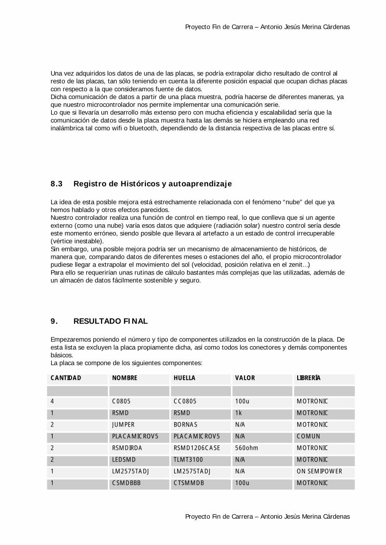
Figura 1: Mochila para transformación de 12V a 1.5V
Figura 2: Placa de acoplo entre microprocesador Motorola y PIC
Proyecto Fin de Carrera – Antonio Jesús Merina Cárdenas
Proyecto Fin de Carrera – Antonio Jesús Merina Cárdenas
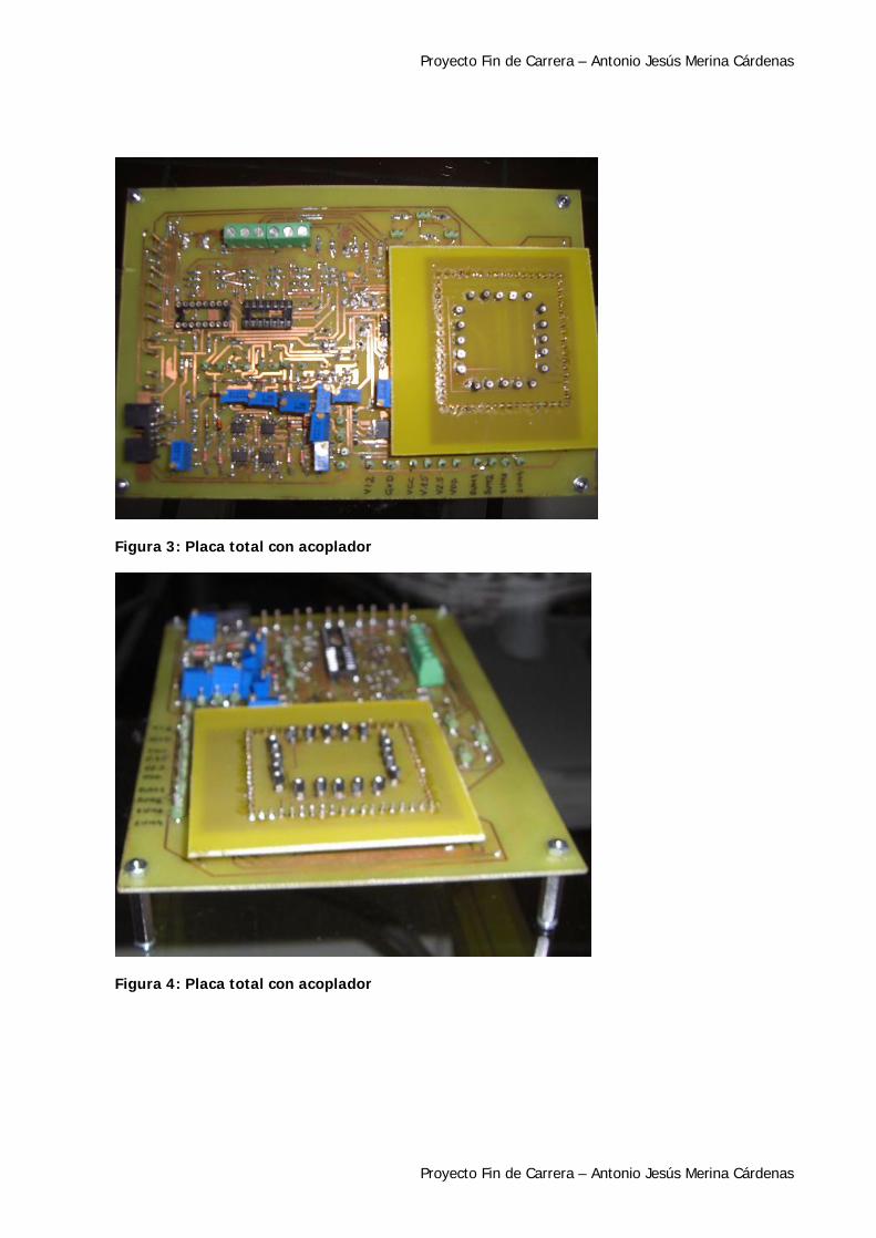
Figura 3: Placa total con acoplador
Figura 4: Placa total con acoplador
Proyecto Fin de Carrera – Antonio Jesús Merina Cárdenas
Proyecto Fin de Carrera – Antonio Jesús Merina Cárdenas
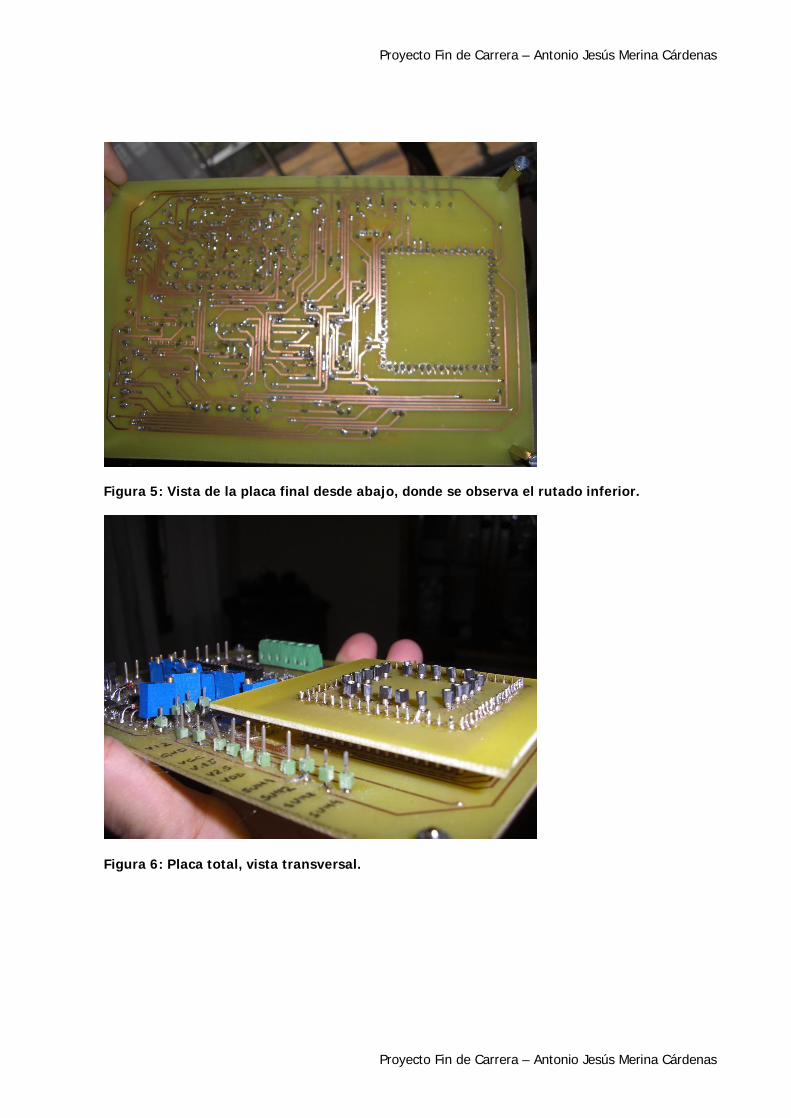
Figura 5: Vista de la placa final desde abajo, donde se observa el rutado inferior.
Figura 6: Placa total, vista transversal.

Proyecto Fin de Carrera – Antonio Jesús Merina Cárdenas
Proyecto Fin de Carrera – Antonio Jesús Merina Cárdenas
10. ANEXOS: Aquí se adjuntan los datasheet de los distintos componentes que componen el montaje:
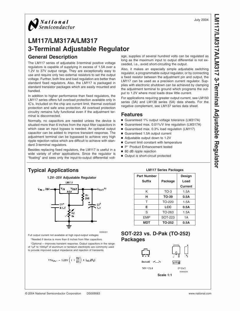
LM117/LM317A/LM3173-Terminal Adjustable RegulatorGeneral DescriptionThe LM117 series of adjustable 3-terminal positive voltageregulators is capable of supplying in excess of 1.5A over a1.2V to 37V output range. They are exceptionally easy touse and require only two external resistors to set the outputvoltage. Further, both line and load regulation are better thanstandard fixed regulators. Also, the LM117 is packaged instandard transistor packages which are easily mounted andhandled.
In addition to higher performance than fixed regulators, theLM117 series offers full overload protection available only inIC’s. Included on the chip are current limit, thermal overloadprotection and safe area protection. All overload protectioncircuitry remains fully functional even if the adjustment ter-minal is disconnected.
Normally, no capacitors are needed unless the device issituated more than 6 inches from the input filter capacitors inwhich case an input bypass is needed. An optional outputcapacitor can be added to improve transient response. Theadjustment terminal can be bypassed to achieve very highripple rejection ratios which are difficult to achieve with stan-dard 3-terminal regulators.
Besides replacing fixed regulators, the LM117 is useful in awide variety of other applications. Since the regulator is“floating” and sees only the input-to-output differential volt-
age, supplies of several hundred volts can be regulated aslong as the maximum input to output differential is not ex-ceeded, i.e., avoid short-circuiting the output.
Also, it makes an especially simple adjustable switchingregulator, a programmable output regulator, or by connectinga fixed resistor between the adjustment pin and output, theLM117 can be used as a precision current regulator. Sup-plies with electronic shutdown can be achieved by clampingthe adjustment terminal to ground which programs the out-put to 1.2V where most loads draw little current.
For applications requiring greater output current, see LM150series (3A) and LM138 series (5A) data sheets. For thenegative complement, see LM137 series data sheet.
Featuresn Guaranteed 1% output voltage tolerance (LM317A)n Guaranteed max. 0.01%/V line regulation (LM317A)n Guaranteed max. 0.3% load regulation (LM117)n Guaranteed 1.5A output currentn Adjustable output down to 1.2Vn Current limit constant with temperaturen P+ Product Enhancement testedn 80 dB ripple rejectionn Output is short-circuit protected
Typical Applications1.2V–25V Adjustable Regulator
00906301
Full output current not available at high input-output voltages
*Needed if device is more than 6 inches from filter capacitors.
†Optional — improves transient response. Output capacitors in the rangeof 1µF to 1000µF of aluminum or tantalum electrolytic are commonly usedto provide improved output impedance and rejection of transients.
LM117 Series Packages
Part Number Design
Suffix Package Load
Current
K TO-3 1.5A
H TO-39 0.5A
T TO-220 1.5A
E LCC 0.5A
S TO-263 1.5A
EMP SOT-223 1A
MDT TO-252 0.5A
SOT-223 vs. D-Pak (TO-252)Packages
00906354
Scale 1:1
July 2004LM
117/LM317A
/LM317
3-TerminalA
djustableR
egulator
© 2004 National Semiconductor Corporation DS009063 www.national.com
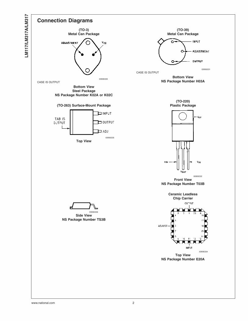
Connection Diagrams
(TO-3)Metal Can Package
(TO-39)Metal Can Package
00906330
CASE IS OUTPUT
Bottom ViewSteel Package
NS Package Number K02A or K02C
00906331
CASE IS OUTPUT
Bottom ViewNS Package Number H03A
(TO-263) Surface-Mount Package(TO-220)
Plastic Package
00906335
Top View
00906332
Front ViewNS Package Number T03B
Ceramic LeadlessChip Carrier
00906336
Side ViewNS Package Number TS3B
00906334
Top ViewNS Package Number E20A
LM11
7/LM
317A
/LM
317
www.national.com 2
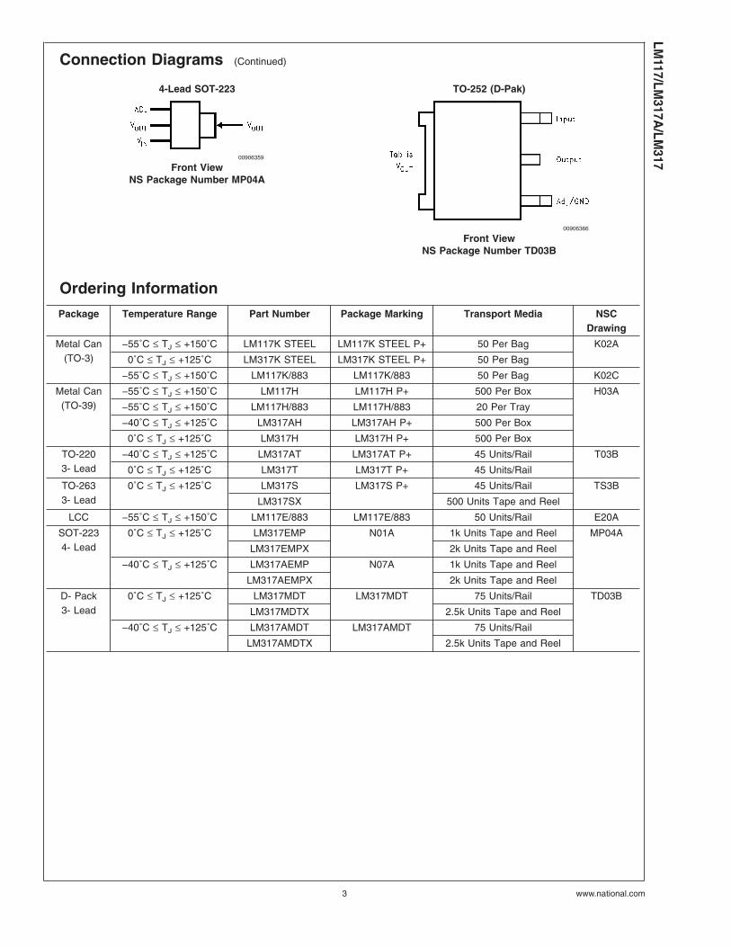
Connection Diagrams (Continued)
4-Lead SOT-223 TO-252 (D-Pak)
00906359
Front ViewNS Package Number MP04A
00906366
Front ViewNS Package Number TD03B
Ordering Information
Package Temperature Range Part Number Package Marking Transport Media NSCDrawing
Metal Can(TO-3)
−55˚C ≤ TJ ≤ +150˚C LM117K STEEL LM117K STEEL P+ 50 Per Bag K02A
0˚C ≤ TJ ≤ +125˚C LM317K STEEL LM317K STEEL P+ 50 Per Bag
−55˚C ≤ TJ ≤ +150˚C LM117K/883 LM117K/883 50 Per Bag K02C
Metal Can(TO-39)
−55˚C ≤ TJ ≤ +150˚C LM117H LM117H P+ 500 Per Box H03A
−55˚C ≤ TJ ≤ +150˚C LM117H/883 LM117H/883 20 Per Tray
−40˚C ≤ TJ ≤ +125˚C LM317AH LM317AH P+ 500 Per Box
0˚C ≤ TJ ≤ +125˚C LM317H LM317H P+ 500 Per Box
TO-2203- Lead
−40˚C ≤ TJ ≤ +125˚C LM317AT LM317AT P+ 45 Units/Rail T03B
0˚C ≤ TJ ≤ +125˚C LM317T LM317T P+ 45 Units/Rail
TO-2633- Lead
0˚C ≤ TJ ≤ +125˚C LM317S LM317S P+ 45 Units/Rail TS3B
LM317SX 500 Units Tape and Reel
LCC −55˚C ≤ TJ ≤ +150˚C LM117E/883 LM117E/883 50 Units/Rail E20A
SOT-2234- Lead
0˚C ≤ TJ ≤ +125˚C LM317EMP N01A 1k Units Tape and Reel MP04A
LM317EMPX 2k Units Tape and Reel
−40˚C ≤ TJ ≤ +125˚C LM317AEMP N07A 1k Units Tape and Reel
LM317AEMPX 2k Units Tape and Reel
D- Pack3- Lead
0˚C ≤ TJ ≤ +125˚C LM317MDT LM317MDT 75 Units/Rail TD03B
LM317MDTX 2.5k Units Tape and Reel
−40˚C ≤ TJ ≤ +125˚C LM317AMDT LM317AMDT 75 Units/Rail
LM317AMDTX 2.5k Units Tape and Reel
LM117/LM
317A/LM
317
www.national.com3
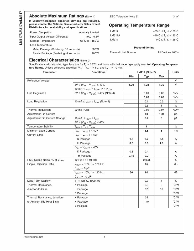
Absolute Maximum Ratings (Note 1)
If Military/Aerospace specified devices are required,please contact the National Semiconductor Sales Office/Distributors for availability and specifications.
Power Dissipation Internally Limited
Input-Output Voltage Differential +40V, −0.3V
Storage Temperature −65˚C to +150˚C
Lead Temperature
Metal Package (Soldering, 10 seconds) 300˚C
Plastic Package (Soldering, 4 seconds) 260˚C
ESD Tolerance (Note 5) 3 kV
Operating Temperature RangeLM117 −55˚C ≤ TJ ≤ +150˚C
LM317A −40˚C ≤ TJ ≤ +125˚C
LM317 0˚C ≤ TJ ≤ +125˚C
Preconditioning
Thermal Limit Burn-In All Devices 100%
Electrical Characteristics (Note 3)
Specifications with standard type face are for TJ = 25˚C, and those with boldface type apply over full Operating Tempera-ture Range. Unless otherwise specified, VIN − VOUT = 5V, and IOUT = 10 mA.
Parameter Conditions LM117 (Note 2) Units
Min Typ Max
Reference Voltage V
3V ≤ (VIN − VOUT) ≤ 40V, 1.20 1.25 1.30 V
10 mA ≤ IOUT ≤ IMAX, P ≤ PMAX
Line Regulation 3V ≤ (VIN − VOUT) ≤ 40V (Note 4) 0.01 0.02 %/V
0.02 0.05 %/V
Load Regulation 10 mA ≤ IOUT ≤ IMAX (Note 4) 0.1 0.3 %
0.3 1 %
Thermal Regulation 20 ms Pulse 0.03 0.07 %/W
Adjustment Pin Current 50 100 µA
Adjustment Pin Current Change 10 mA ≤ IOUT ≤ IMAX 0.2 5 µA
3V ≤ (VIN − VOUT) ≤ 40V
Temperature Stability TMIN ≤ TJ ≤ TMAX 1 %
Minimum Load Current (VIN − VOUT) = 40V 3.5 5 mA
Current Limit (VIN − VOUT) ≤ 15V
K Package 1.5 2.2 3.4 A
H Package 0.5 0.8 1.8 A
(VIN − VOUT) = 40V
K Package 0.3 0.4 A
H Package 0.15 0.2 A
RMS Output Noise, % of VOUT 10 Hz ≤ f ≤ 10 kHz 0.003 %
Ripple Rejection Ratio VOUT = 10V, f = 120 Hz, 65 dB
CADJ = 0 µF
VOUT = 10V, f = 120 Hz, 66 80 dB
CADJ = 10 µF
Long-Term Stability TJ = 125˚C, 1000 hrs 0.3 1 %
Thermal Resistance, K Package 2.3 3 ˚C/W
Junction-to-Case H Package 12 15 ˚C/W
E Package ˚C/W
Thermal Resistance, Junction- K Package 35 ˚C/W
to-Ambient (No Heat Sink) H Package 140 ˚C/W
E Package ˚C/W
LM11
7/LM
317A
/LM
317
www.national.com 4
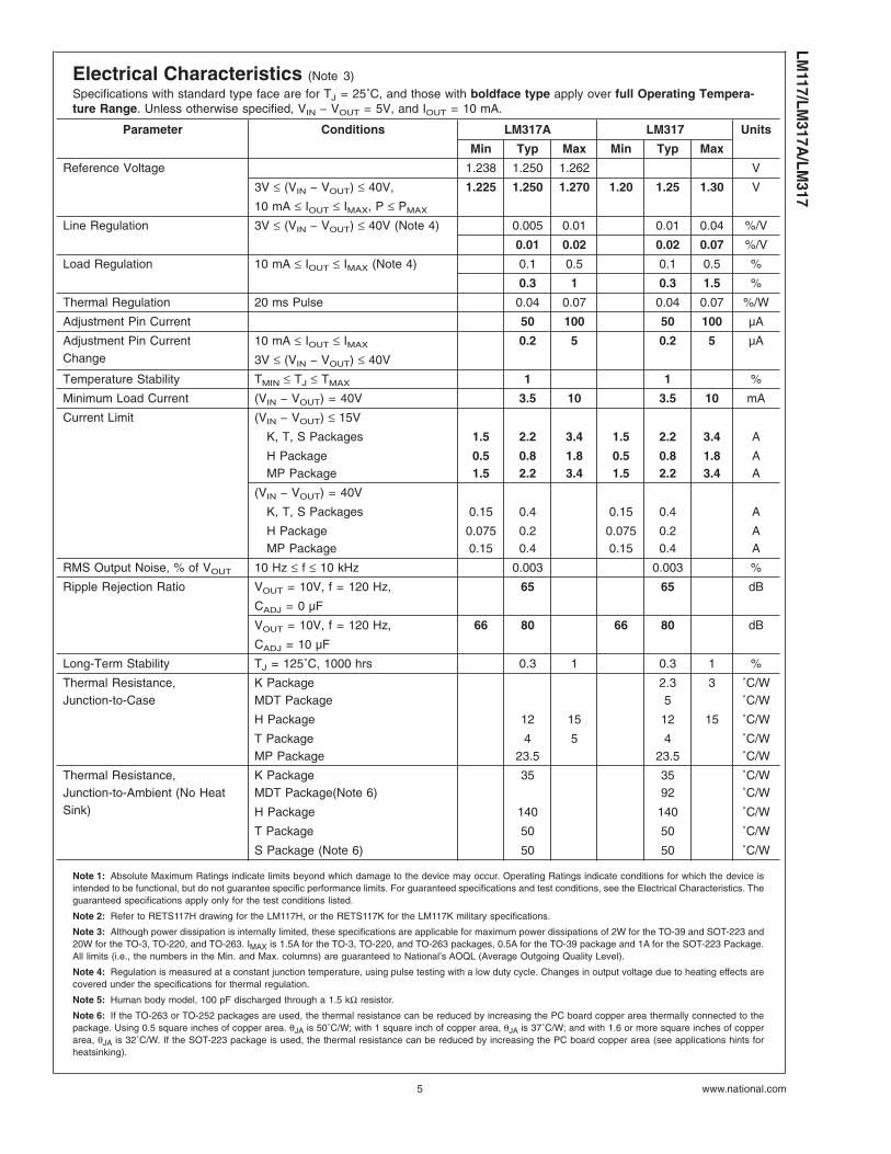
Electrical Characteristics (Note 3)
Specifications with standard type face are for TJ = 25˚C, and those with boldface type apply over full Operating Tempera-ture Range. Unless otherwise specified, VIN − VOUT = 5V, and IOUT = 10 mA.
Parameter Conditions LM317A LM317 Units
Min Typ Max Min Typ Max
Reference Voltage 1.238 1.250 1.262 V
3V ≤ (VIN − VOUT) ≤ 40V, 1.225 1.250 1.270 1.20 1.25 1.30 V
10 mA ≤ IOUT ≤ IMAX, P ≤ PMAX
Line Regulation 3V ≤ (VIN − VOUT) ≤ 40V (Note 4) 0.005 0.01 0.01 0.04 %/V
0.01 0.02 0.02 0.07 %/V
Load Regulation 10 mA ≤ IOUT ≤ IMAX (Note 4) 0.1 0.5 0.1 0.5 %
0.3 1 0.3 1.5 %
Thermal Regulation 20 ms Pulse 0.04 0.07 0.04 0.07 %/W
Adjustment Pin Current 50 100 50 100 µA
Adjustment Pin CurrentChange
10 mA ≤ IOUT ≤ IMAX 0.2 5 0.2 5 µA
3V ≤ (VIN − VOUT) ≤ 40V
Temperature Stability TMIN ≤ TJ ≤ TMAX 1 1 %
Minimum Load Current (VIN − VOUT) = 40V 3.5 10 3.5 10 mA
Current Limit (VIN − VOUT) ≤ 15V
K, T, S Packages 1.5 2.2 3.4 1.5 2.2 3.4 A
H PackageMP Package
0.51.5
0.82.2
1.83.4
0.51.5
0.82.2
1.83.4
AA
(VIN − VOUT) = 40V
K, T, S Packages 0.15 0.4 0.15 0.4 A
H PackageMP Package
0.0750.15
0.20.4
0.0750.15
0.20.4
AA
RMS Output Noise, % of VOUT 10 Hz ≤ f ≤ 10 kHz 0.003 0.003 %
Ripple Rejection Ratio VOUT = 10V, f = 120 Hz, 65 65 dB
CADJ = 0 µF
VOUT = 10V, f = 120 Hz, 66 80 66 80 dB
CADJ = 10 µF
Long-Term Stability TJ = 125˚C, 1000 hrs 0.3 1 0.3 1 %
Thermal Resistance,Junction-to-Case
K PackageMDT Package
2.35
3 ˚C/W˚C/W
H Package 12 15 12 15 ˚C/W
T PackageMP Package
423.5
5 423.5
˚C/W˚C/W
Thermal Resistance,Junction-to-Ambient (No HeatSink)
K PackageMDT Package(Note 6)
35 3592
˚C/W˚C/W
H Package 140 140 ˚C/W
T Package 50 50 ˚C/W
S Package (Note 6) 50 50 ˚C/W
Note 1: Absolute Maximum Ratings indicate limits beyond which damage to the device may occur. Operating Ratings indicate conditions for which the device isintended to be functional, but do not guarantee specific performance limits. For guaranteed specifications and test conditions, see the Electrical Characteristics. Theguaranteed specifications apply only for the test conditions listed.
Note 2: Refer to RETS117H drawing for the LM117H, or the RETS117K for the LM117K military specifications.
Note 3: Although power dissipation is internally limited, these specifications are applicable for maximum power dissipations of 2W for the TO-39 and SOT-223 and20W for the TO-3, TO-220, and TO-263. IMAX is 1.5A for the TO-3, TO-220, and TO-263 packages, 0.5A for the TO-39 package and 1A for the SOT-223 Package.All limits (i.e., the numbers in the Min. and Max. columns) are guaranteed to National’s AOQL (Average Outgoing Quality Level).
Note 4: Regulation is measured at a constant junction temperature, using pulse testing with a low duty cycle. Changes in output voltage due to heating effects arecovered under the specifications for thermal regulation.
Note 5: Human body model, 100 pF discharged through a 1.5 kΩ resistor.
Note 6: If the TO-263 or TO-252 packages are used, the thermal resistance can be reduced by increasing the PC board copper area thermally connected to thepackage. Using 0.5 square inches of copper area. θJA is 50˚C/W; with 1 square inch of copper area, θJA is 37˚C/W; and with 1.6 or more square inches of copperarea, θJA is 32˚C/W. If the SOT-223 package is used, the thermal resistance can be reduced by increasing the PC board copper area (see applications hints forheatsinking).
LM117/LM
317A/LM
317
www.national.com5
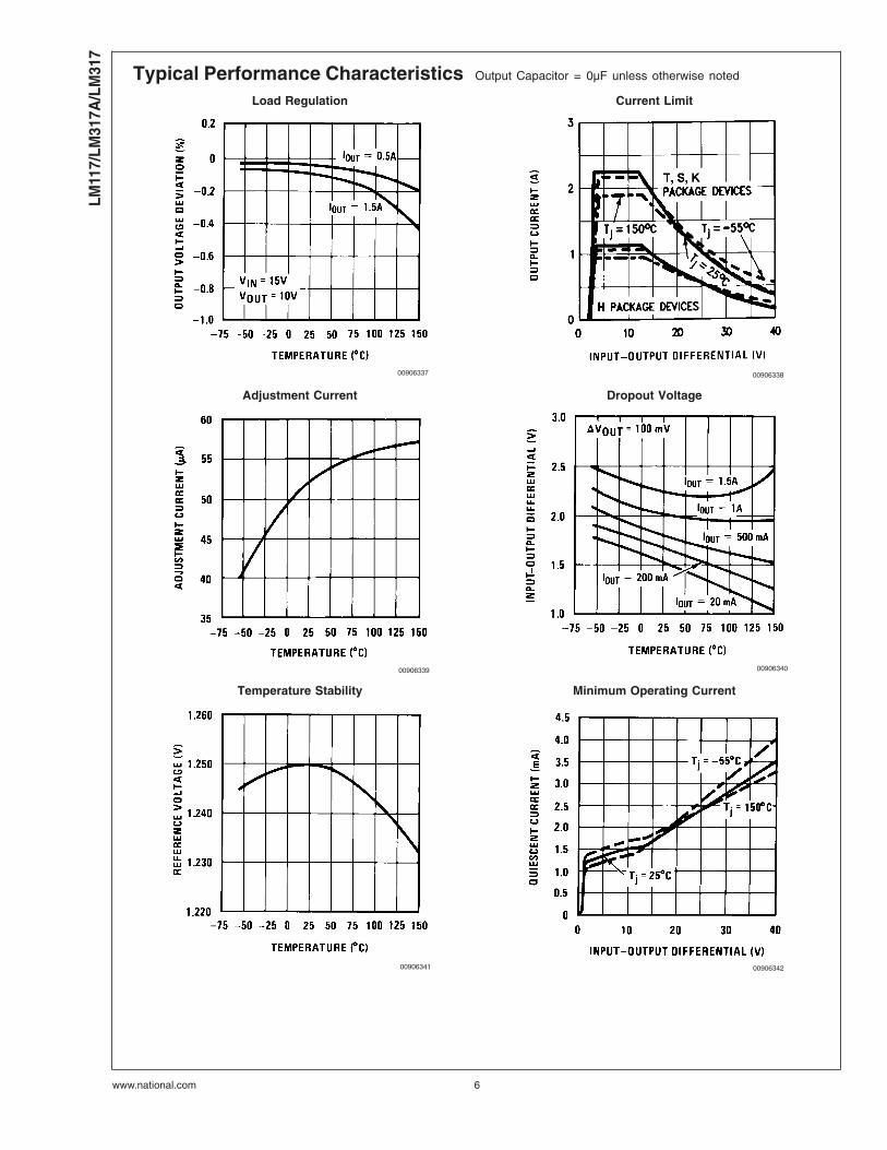
Typical Performance Characteristics Output Capacitor = 0µF unless otherwise noted
Load Regulation Current Limit
00906337 00906338
Adjustment Current Dropout Voltage
00906339 00906340
Temperature Stability Minimum Operating Current
00906341 00906342
LM11
7/LM
317A
/LM
317
www.national.com 6
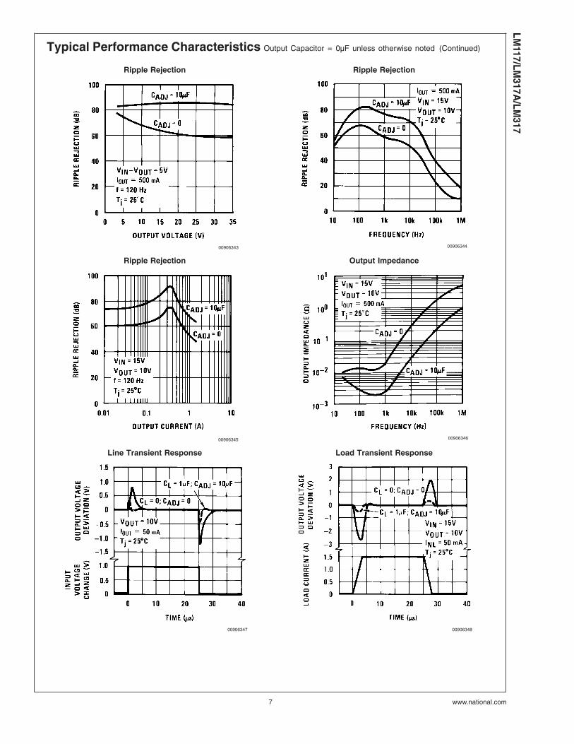
Typical Performance Characteristics Output Capacitor = 0µF unless otherwise noted (Continued)
Ripple Rejection Ripple Rejection
00906343 00906344
Ripple Rejection Output Impedance
00906345 00906346
Line Transient Response Load Transient Response
00906347 00906348
LM117/LM
317A/LM
317
www.national.com7
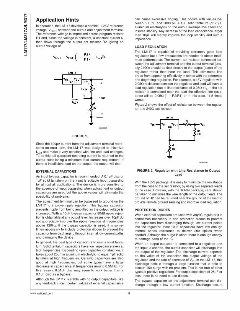
Application HintsIn operation, the LM117 develops a nominal 1.25V referencevoltage, VREF, between the output and adjustment terminal.The reference voltage is impressed across program resistorR1 and, since the voltage is constant, a constant current I1then flows through the output set resistor R2, giving anoutput voltage of
Since the 100µA current from the adjustment terminal repre-sents an error term, the LM117 was designed to minimizeIADJ and make it very constant with line and load changes.To do this, all quiescent operating current is returned to theoutput establishing a minimum load current requirement. Ifthere is insufficient load on the output, the output will rise.
EXTERNAL CAPACITORS
An input bypass capacitor is recommended. A 0.1µF disc or1µF solid tantalum on the input is suitable input bypassingfor almost all applications. The device is more sensitive tothe absence of input bypassing when adjustment or outputcapacitors are used but the above values will eliminate thepossibility of problems.
The adjustment terminal can be bypassed to ground on theLM117 to improve ripple rejection. This bypass capacitorprevents ripple from being amplified as the output voltage isincreased. With a 10µF bypass capacitor 80dB ripple rejec-tion is obtainable at any output level. Increases over 10µF donot appreciably improve the ripple rejection at frequenciesabove 120Hz. If the bypass capacitor is used, it is some-times necessary to include protection diodes to prevent thecapacitor from discharging through internal low current pathsand damaging the device.
In general, the best type of capacitors to use is solid tanta-lum. Solid tantalum capacitors have low impedance even athigh frequencies. Depending upon capacitor construction, ittakes about 25µF in aluminum electrolytic to equal 1µF solidtantalum at high frequencies. Ceramic capacitors are alsogood at high frequencies; but some types have a largedecrease in capacitance at frequencies around 0.5MHz. Forthis reason, 0.01µF disc may seem to work better than a0.1µF disc as a bypass.
Although the LM117 is stable with no output capacitors, likeany feedback circuit, certain values of external capacitance
can cause excessive ringing. This occurs with values be-tween 500 pF and 5000 pF. A 1µF solid tantalum (or 25µFaluminum electrolytic) on the output swamps this effect andinsures stability. Any increase of the load capacitance largerthan 10µF will merely improve the loop stability and outputimpedance.
LOAD REGULATION
The LM117 is capable of providing extremely good loadregulation but a few precautions are needed to obtain maxi-mum performance. The current set resistor connected be-tween the adjustment terminal and the output terminal (usu-ally 240Ω) should be tied directly to the output (case) of theregulator rather than near the load. This eliminates linedrops from appearing effectively in series with the referenceand degrading regulation. For example, a 15V regulator with0.05Ω resistance between the regulator and load will have aload regulation due to line resistance of 0.05Ω x IL. If the setresistor is connected near the load the effective line resis-tance will be 0.05Ω (1 + R2/R1) or in this case, 11.5 timesworse.
Figure 2 shows the effect of resistance between the regula-tor and 240Ω set resistor.
With the TO-3 package, it is easy to minimize the resistancefrom the case to the set resistor, by using two separate leadsto the case. However, with the TO-39 package, care shouldbe taken to minimize the wire length of the output lead. Theground of R2 can be returned near the ground of the load toprovide remote ground sensing and improve load regulation.
PROTECTION DIODES
When external capacitors are used with any IC regulator it issometimes necessary to add protection diodes to preventthe capacitors from discharging through low current pointsinto the regulator. Most 10µF capacitors have low enoughinternal series resistance to deliver 20A spikes whenshorted. Although the surge is short, there is enough energyto damage parts of the IC.
When an output capacitor is connected to a regulator andthe input is shorted, the output capacitor will discharge intothe output of the regulator. The discharge current dependson the value of the capacitor, the output voltage of theregulator, and the rate of decrease of VIN. In the LM117, thisdischarge path is through a large junction that is able tosustain 15A surge with no problem. This is not true of othertypes of positive regulators. For output capacitors of 25µF orless, there is no need to use diodes.
The bypass capacitor on the adjustment terminal can dis-charge through a low current junction. Discharge occurs
00906305
FIGURE 1.
00906306
FIGURE 2. Regulator with Line Resistance in OutputLead
LM11
7/LM
317A
/LM
317
www.national.com 8

Application Hints (Continued)
when either the input or output is shorted. Internal to theLM117 is a 50Ω resistor which limits the peak dischargecurrent. No protection is needed for output voltages of 25Vor less and 10µF capacitance. Figure 3 shows an LM117with protection diodes included for use with outputs greaterthan 25V and high values of output capacitance.
When a value for θ(H−A) is found using the equation shown,a heatsink must be selected that has a value that is less thanor equal to this number.
θ(H−A) is specified numerically by the heatsink manufacturerin the catalog, or shown in a curve that plots temperature risevs power dissipation for the heatsink.
HEATSINKING TO-263, SOT-223 AND TO-252 PACKAGEPARTS
The TO-263 (“S”), SOT-223 (“MP”) and TO-252 (”DT”) pack-ages use a copper plane on the PCB and the PCB itself asa heatsink. To optimize the heat sinking ability of the planeand PCB, solder the tab of the package to the plane.
Figure 4 shows for the TO-263 the measured values of θ(J−A)
for different copper area sizes using a typical PCB with 1ounce copper and no solder mask over the copper area usedfor heatsinking.
As shown in the figure, increasing the copper area beyond 1square inch produces very little improvement. It should alsobe observed that the minimum value of θ(J−A) for the TO-263package mounted to a PCB is 32˚C/W.
As a design aid, Figure 5 shows the maximum allowablepower dissipation compared to ambient temperature for theTO-263 device (assuming θ(J−A) is 35˚C/W and the maxi-mum junction temperature is 125˚C).
Figure 6 and Figure 7 show the information for the SOT-223package. Figure 7 assumes a θ(J−A) of 74˚C/W for 1 ouncecopper and 51˚C/W for 2 ounce copper and a maximumjunction temperature of 125˚C.
00906307
D1 protects against C1
D2 protects against C2
FIGURE 3. Regulator with Protection Diodes
00906355
FIGURE 4. θ(J−A) vs Copper (1 ounce) Area for theTO-263 Package
00906356
FIGURE 5. Maximum Power Dissipation vs TAMB forthe TO-263 Package
LM117/LM
317A/LM
317
www.national.com9
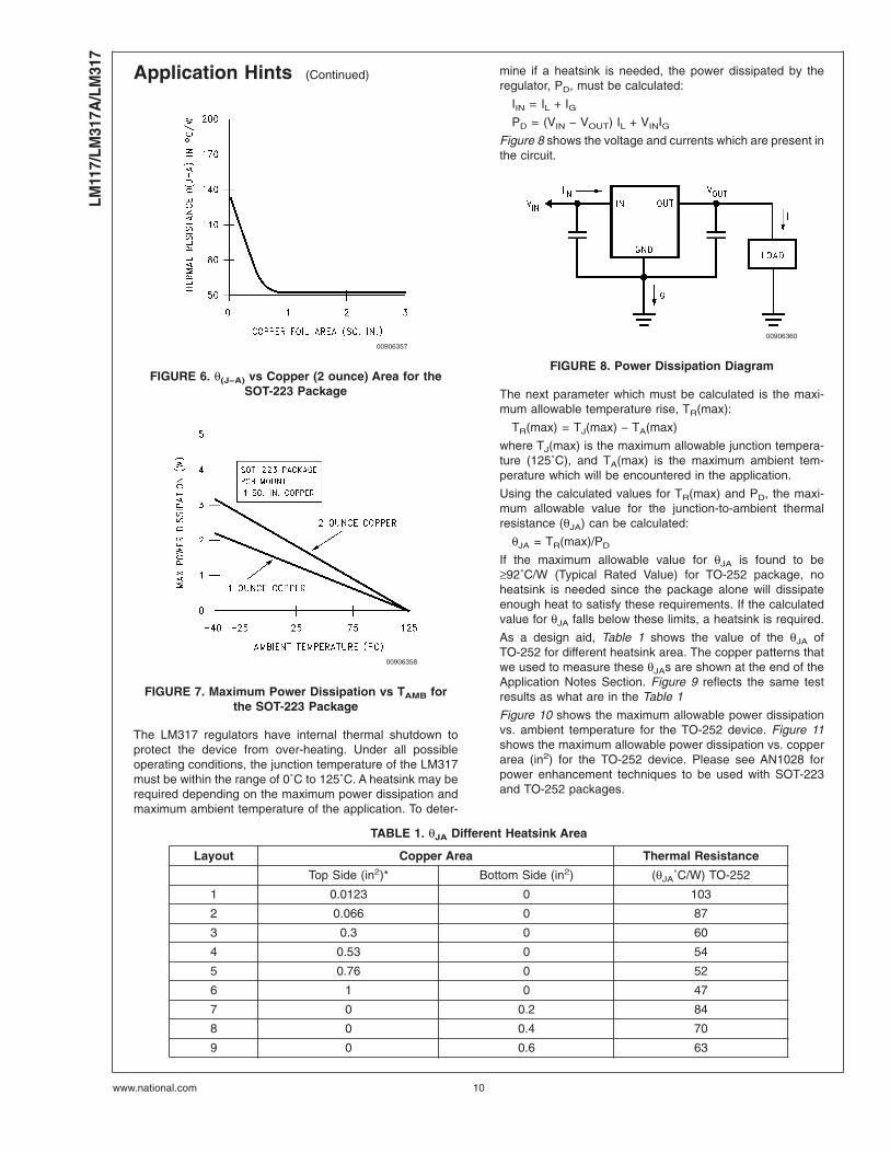
Application Hints (Continued)
The LM317 regulators have internal thermal shutdown toprotect the device from over-heating. Under all possibleoperating conditions, the junction temperature of the LM317must be within the range of 0˚C to 125˚C. A heatsink may berequired depending on the maximum power dissipation andmaximum ambient temperature of the application. To deter-
mine if a heatsink is needed, the power dissipated by theregulator, PD, must be calculated:
IIN = IL + IGPD = (VIN − VOUT) IL + VINIG
Figure 8 shows the voltage and currents which are present inthe circuit.
The next parameter which must be calculated is the maxi-mum allowable temperature rise, TR(max):
TR(max) = TJ(max) − TA(max)
where TJ(max) is the maximum allowable junction tempera-ture (125˚C), and TA(max) is the maximum ambient tem-perature which will be encountered in the application.
Using the calculated values for TR(max) and PD, the maxi-mum allowable value for the junction-to-ambient thermalresistance (θJA) can be calculated:
θJA = TR(max)/PD
If the maximum allowable value for θJA is found to be≥92˚C/W (Typical Rated Value) for TO-252 package, noheatsink is needed since the package alone will dissipateenough heat to satisfy these requirements. If the calculatedvalue for θJA falls below these limits, a heatsink is required.
As a design aid, Table 1 shows the value of the θJA ofTO-252 for different heatsink area. The copper patterns thatwe used to measure these θJAs are shown at the end of theApplication Notes Section. Figure 9 reflects the same testresults as what are in the Table 1
Figure 10 shows the maximum allowable power dissipationvs. ambient temperature for the TO-252 device. Figure 11shows the maximum allowable power dissipation vs. copperarea (in2) for the TO-252 device. Please see AN1028 forpower enhancement techniques to be used with SOT-223and TO-252 packages.
TABLE 1. θJA Different Heatsink Area
Layout Copper Area Thermal Resistance
Top Side (in2)* Bottom Side (in2) (θJA˚C/W) TO-252
1 0.0123 0 103
2 0.066 0 87
3 0.3 0 60
4 0.53 0 54
5 0.76 0 52
6 1 0 47
7 0 0.2 84
8 0 0.4 70
9 0 0.6 63
00906357
FIGURE 6. θ(J−A) vs Copper (2 ounce) Area for theSOT-223 Package
00906358
FIGURE 7. Maximum Power Dissipation vs TAMB forthe SOT-223 Package
00906360
FIGURE 8. Power Dissipation Diagram
LM11
7/LM
317A
/LM
317
www.national.com 10
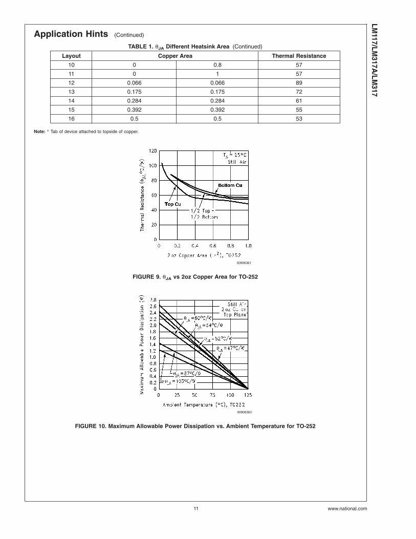
Application Hints (Continued)
TABLE 1. θJA Different Heatsink Area (Continued)
Layout Copper Area Thermal Resistance
10 0 0.8 57
11 0 1 57
12 0.066 0.066 89
13 0.175 0.175 72
14 0.284 0.284 61
15 0.392 0.392 55
16 0.5 0.5 53
Note: * Tab of device attached to topside of copper.
00906361
FIGURE 9. θJA vs 2oz Copper Area for TO-252
00906363
FIGURE 10. Maximum Allowable Power Dissipation vs. Ambient Temperature for TO-252
LM117/LM
317A/LM
317
www.national.com11
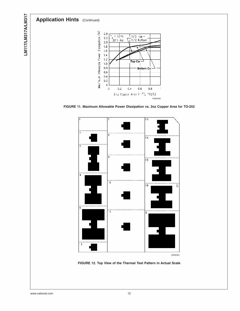
Application Hints (Continued)
00906362
FIGURE 11. Maximum Allowable Power Dissipation vs. 2oz Copper Area for TO-252
00906364
FIGURE 12. Top View of the Thermal Test Pattern in Actual Scale
LM11
7/LM
317A
/LM
317
www.national.com 12
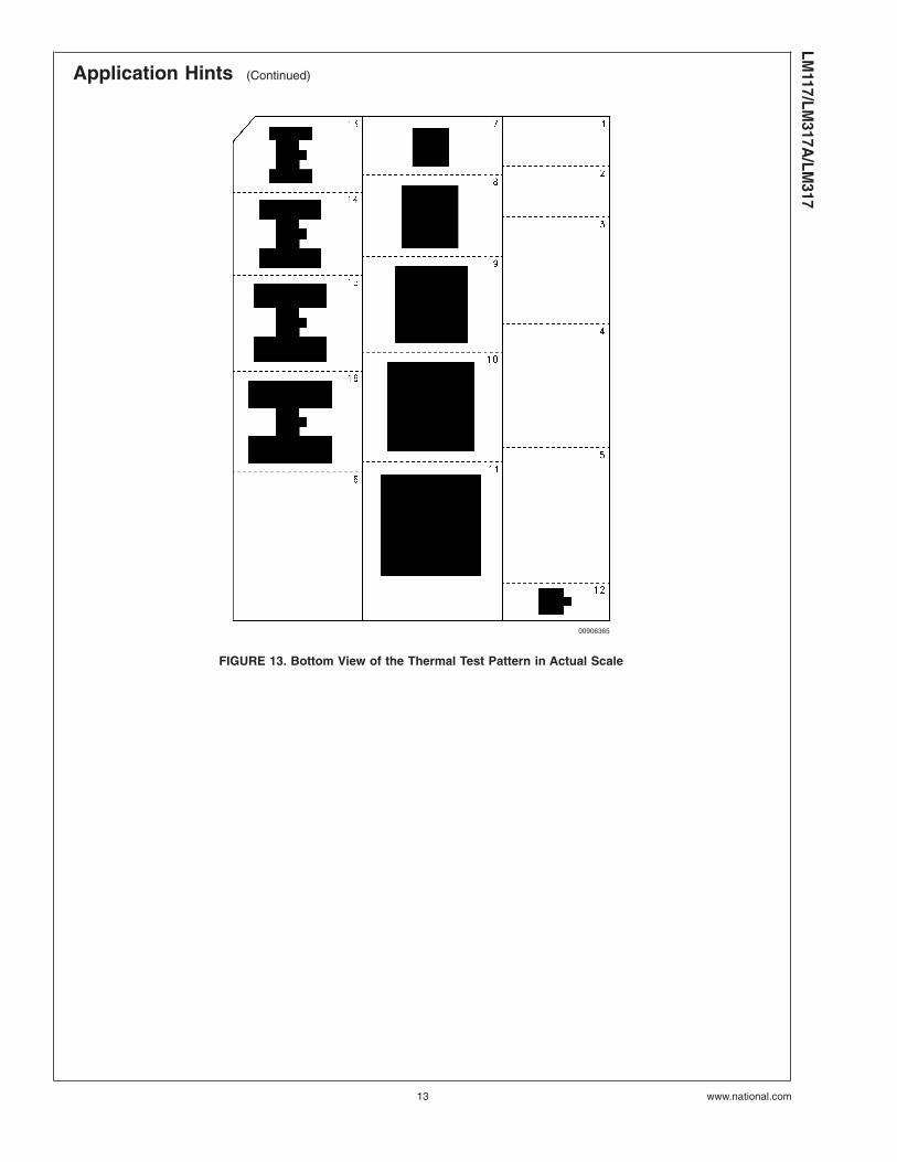
Application Hints (Continued)
00906365
FIGURE 13. Bottom View of the Thermal Test Pattern in Actual Scale
LM117/LM
317A/LM
317
www.national.com13
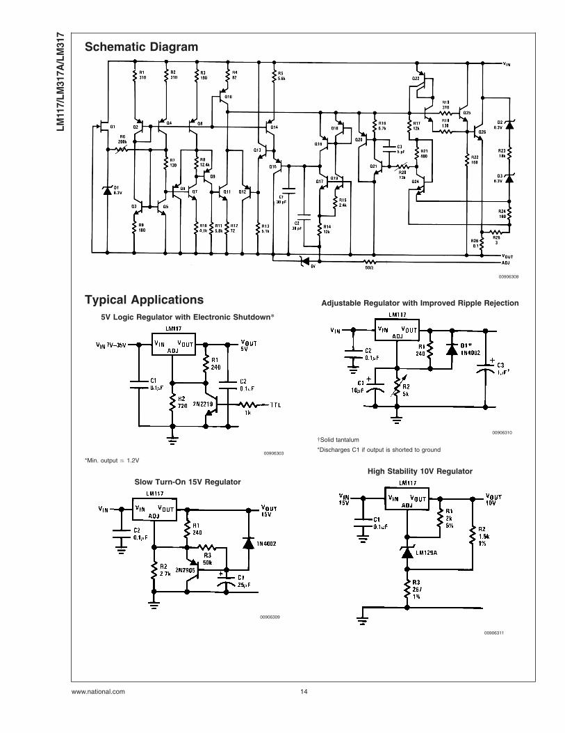
Schematic Diagram
00906308
Typical Applications5V Logic Regulator with Electronic Shutdown*
00906303
*Min. output ) 1.2V
Slow Turn-On 15V Regulator
00906309
Adjustable Regulator with Improved Ripple Rejection
00906310
†Solid tantalum
*Discharges C1 if output is shorted to ground
High Stability 10V Regulator
00906311
LM11
7/LM
317A
/LM
317
www.national.com 14
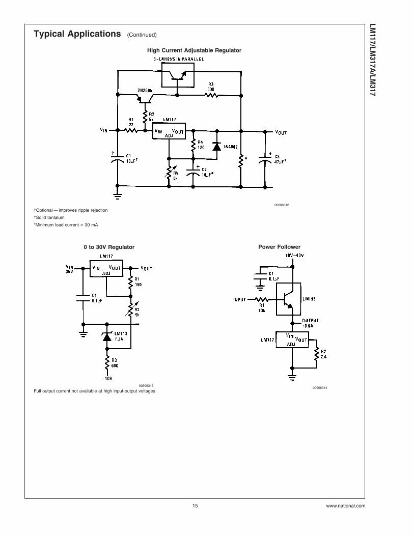
Typical Applications (Continued)
High Current Adjustable Regulator
00906312
‡Optional — improves ripple rejection
†Solid tantalum
*Minimum load current = 30 mA
0 to 30V Regulator
00906313
Full output current not available at high input-output voltages
Power Follower
00906314
LM117/LM
317A/LM
317
www.national.com15
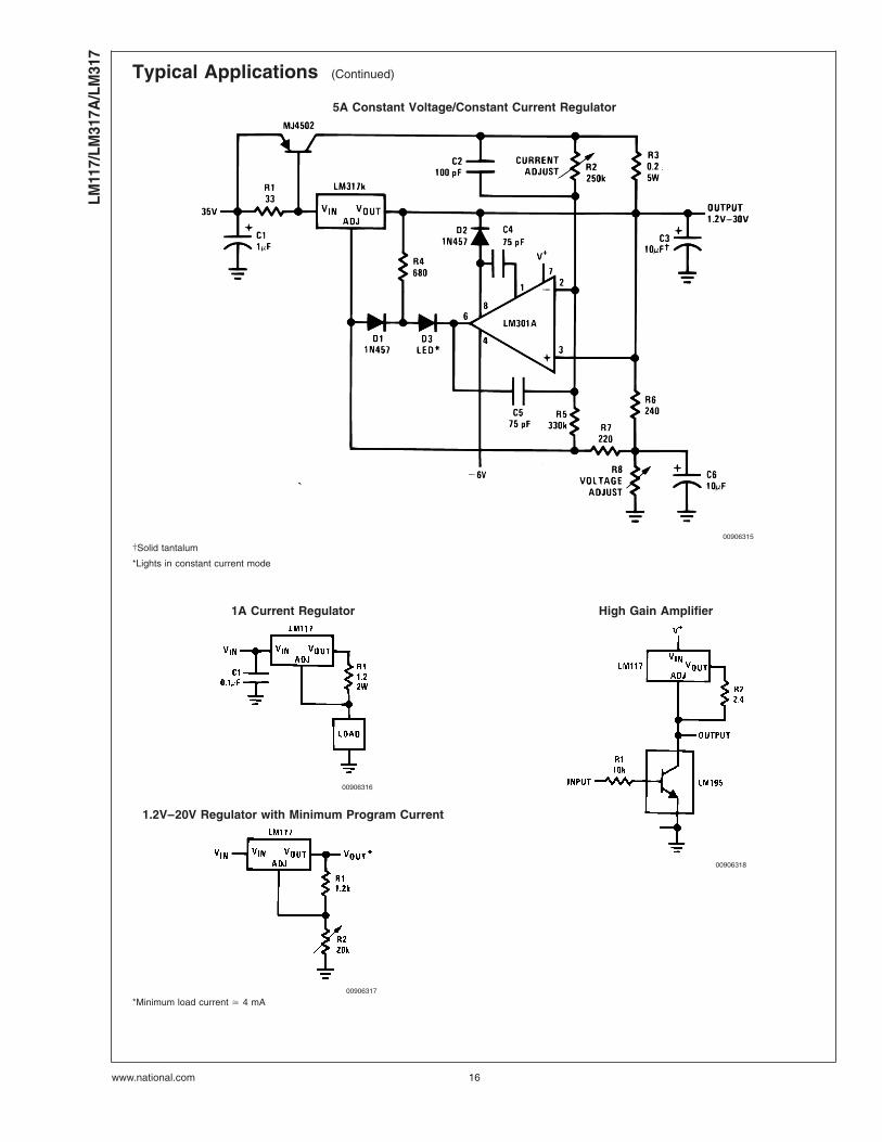
Typical Applications (Continued)
5A Constant Voltage/Constant Current Regulator
00906315
†Solid tantalum
*Lights in constant current mode
1A Current Regulator
00906316
1.2V–20V Regulator with Minimum Program Current
00906317
*Minimum load current ) 4 mA
High Gain Amplifier
00906318
LM11
7/LM
317A
/LM
317
www.national.com 16
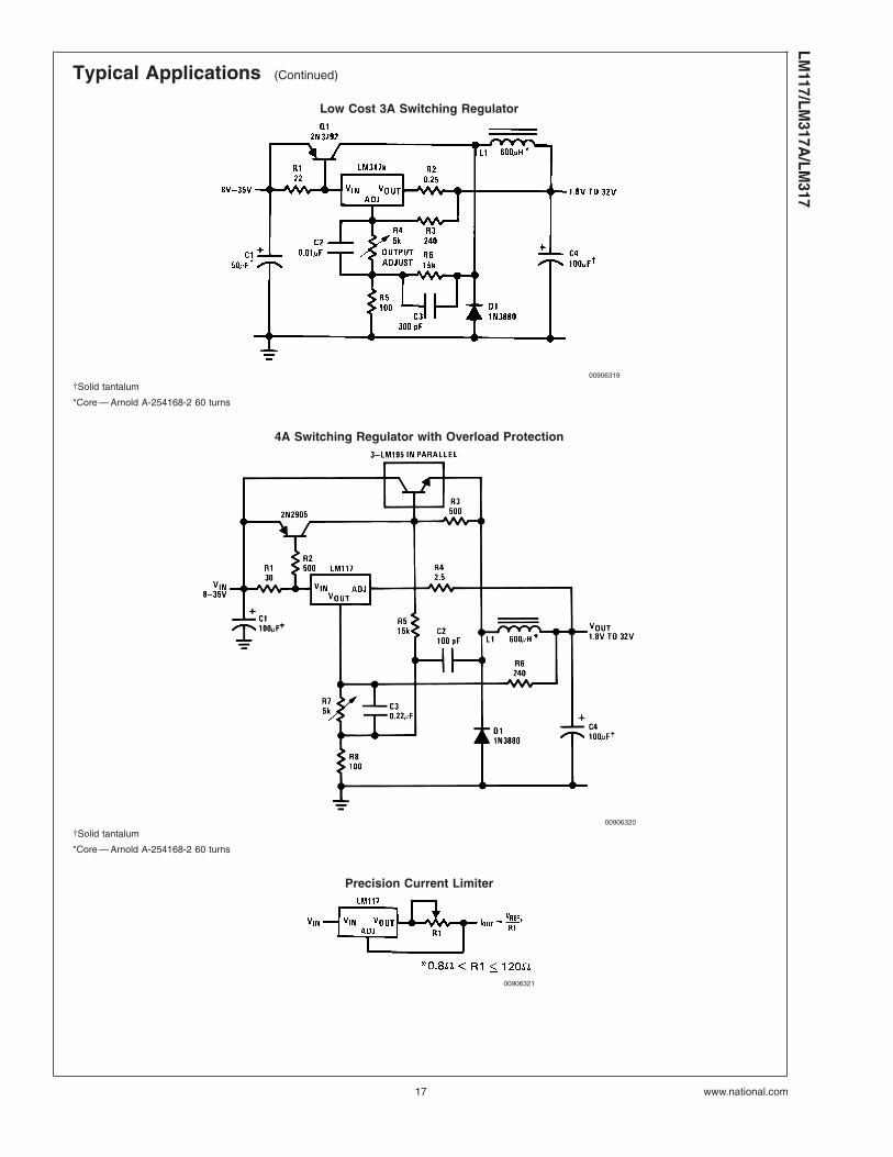
Typical Applications (Continued)
Low Cost 3A Switching Regulator
00906319
†Solid tantalum
*Core — Arnold A-254168-2 60 turns
4A Switching Regulator with Overload Protection
00906320
†Solid tantalum
*Core — Arnold A-254168-2 60 turns
Precision Current Limiter
00906321
LM117/LM
317A/LM
317
www.national.com17
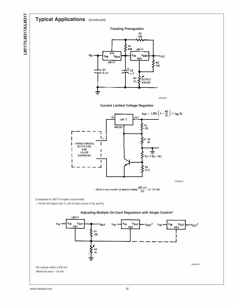
Typical Applications (Continued)
Tracking Preregulator
00906322
Current Limited Voltage Regulator
00906323
(Compared to LM117’s higher current limit)
— At 50 mA output only 3⁄4 volt of drop occurs in R3 and R4
Adjusting Multiple On-Card Regulators with Single Control*
00906324
*All outputs within ±100 mV
†Minimum load — 10 mA
LM11
7/LM
317A
/LM
317
www.national.com 18
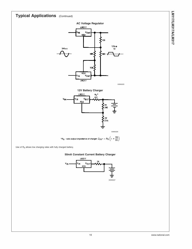
Typical Applications (Continued)
AC Voltage Regulator
00906325
12V Battery Charger
00906326
Use of RS allows low charging rates with fully charged battery.
50mA Constant Current Battery Charger
00906327
LM117/LM
317A/LM
317
www.national.com19
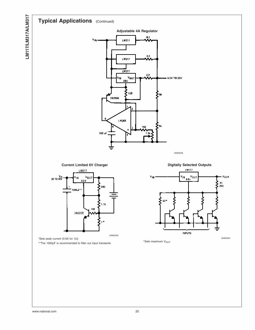
Typical Applications (Continued)
Adjustable 4A Regulator
00906328
Current Limited 6V Charger
00906329
*Sets peak current (0.6A for 1Ω)
**The 1000µF is recommended to filter out input transients
Digitally Selected Outputs
00906302
*Sets maximum VOUT
LM11
7/LM
317A
/LM
317
www.national.com 20
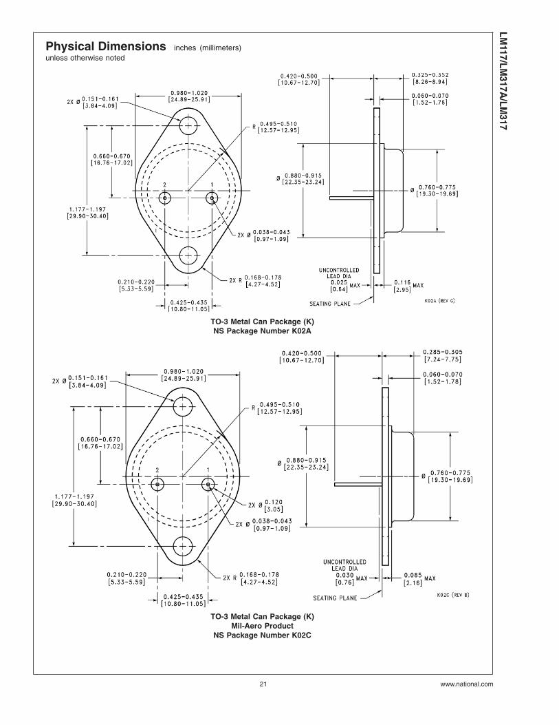
Physical Dimensions inches (millimeters)unless otherwise noted
TO-3 Metal Can Package (K)NS Package Number K02A
TO-3 Metal Can Package (K)Mil-Aero Product
NS Package Number K02C
LM117/LM
317A/LM
317
www.national.com21

Physical Dimensions inches (millimeters) unless otherwise noted (Continued)
(TO-39) Metal Can PackageNS Package Number H03A
3-Lead TO-220NS Package Number T03B
LM11
7/LM
317A
/LM
317
www.national.com 22
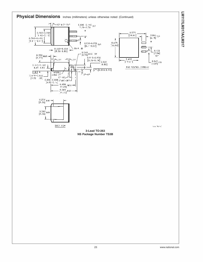
Physical Dimensions inches (millimeters) unless otherwise noted (Continued)
3-Lead TO-263NS Package Number TS3B
LM117/LM
317A/LM
317
www.national.com23
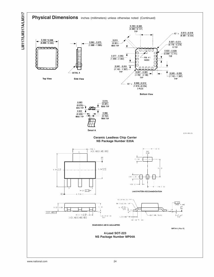
Physical Dimensions inches (millimeters) unless otherwise noted (Continued)
Ceramic Leadless Chip CarrierNS Package Number E20A
4-Lead SOT-223NS Package Number MP04A
LM11
7/LM
317A
/LM
317
www.national.com 24
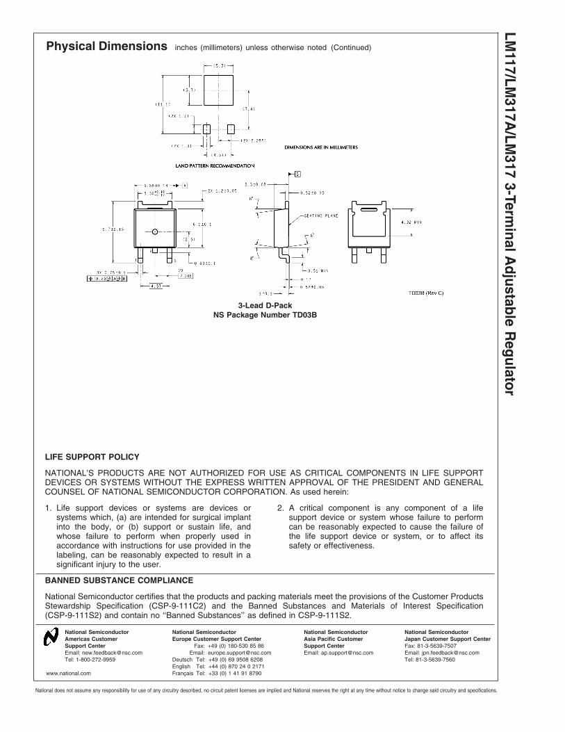
Physical Dimensions inches (millimeters) unless otherwise noted (Continued)
3-Lead D-PackNS Package Number TD03B
LIFE SUPPORT POLICY
NATIONAL’S PRODUCTS ARE NOT AUTHORIZED FOR USE AS CRITICAL COMPONENTS IN LIFE SUPPORTDEVICES OR SYSTEMS WITHOUT THE EXPRESS WRITTEN APPROVAL OF THE PRESIDENT AND GENERALCOUNSEL OF NATIONAL SEMICONDUCTOR CORPORATION. As used herein:
1. Life support devices or systems are devices orsystems which, (a) are intended for surgical implantinto the body, or (b) support or sustain life, andwhose failure to perform when properly used inaccordance with instructions for use provided in thelabeling, can be reasonably expected to result in asignificant injury to the user.
2. A critical component is any component of a lifesupport device or system whose failure to performcan be reasonably expected to cause the failure ofthe life support device or system, or to affect itssafety or effectiveness.
BANNED SUBSTANCE COMPLIANCE
National Semiconductor certifies that the products and packing materials meet the provisions of the Customer ProductsStewardship Specification (CSP-9-111C2) and the Banned Substances and Materials of Interest Specification(CSP-9-111S2) and contain no ‘‘Banned Substances’’ as defined in CSP-9-111S2.
National SemiconductorAmericas CustomerSupport CenterEmail: [email protected]: 1-800-272-9959
National SemiconductorEurope Customer Support Center
Fax: +49 (0) 180-530 85 86Email: [email protected]
Deutsch Tel: +49 (0) 69 9508 6208English Tel: +44 (0) 870 24 0 2171Français Tel: +33 (0) 1 41 91 8790
National SemiconductorAsia Pacific CustomerSupport CenterEmail: [email protected]
National SemiconductorJapan Customer Support CenterFax: 81-3-5639-7507Email: [email protected]: 81-3-5639-7560
www.national.com
LM117/LM
317A/LM
3173-Term
inalAdjustable
Regulator
National does not assume any responsibility for use of any circuitry described, no circuit patent licenses are implied and National reserves the right at any time without notice to change said circuitry and specifications.

This datasheet has been download from:
www.datasheetcatalog.com
Datasheets for electronics components.
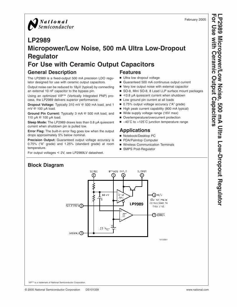
LP2989Micropower/Low Noise, 500 mA Ultra Low-DropoutRegulatorFor Use with Ceramic Output CapacitorsGeneral DescriptionThe LP2989 is a fixed-output 500 mA precision LDO regu-lator designed for use with ceramic output capacitors.
Output noise can be reduced to 18µV (typical) by connectingan external 10 nF capacitor to the bypass pin.
Using an optimized VIP™ (Vertically Integrated PNP) pro-cess, the LP2989 delivers superior performance:
Dropout Voltage: Typically 310 mV @ 500 mA load, and 1mV @ 100 µA load.
Ground Pin Current: Typically 3 mA @ 500 mA load, and110 µA @ 100 µA load.
Sleep Mode: The LP2989 draws less than 0.8 µA quiescentcurrent when shutdown pin is pulled low.
Error Flag: The built-in error flag goes low when the outputdrops approximately 5% below nominal.
Precision Output: Guaranteed output voltage accuracy is0.75% (“A” grade) and 1.25% (standard grade) at roomtemperature.
For output voltages < 2V, see LP2989LV datasheet.
Featuresn Ultra low dropout voltagen Guaranteed 500 mA continuous output currentn Very low output noise with external capacitorn SO-8, Mini SO-8, 8 Lead LLP surface mount packagesn <0.8 µA quiescent current when shutdownn Low ground pin current at all loadsn 0.75% output voltage accuracy (“A” grade)n High peak current capability (800 mA typical)n Wide supply voltage range (16V max)n Overtemperature/overcurrent protectionn −40˚C to +125˚C junction temperature range
Applicationsn Notebook/Desktop PCn PDA/Palmtop Computern Wireless Communication Terminalsn SMPS Post-Regulator
Block Diagram
10133901
VIP™ is a trademark of National Semiconductor Corporation.
February 2005LP
2989M
icropower/Low
Noise,500
mA
Ultra
Low-D
ropoutR
egulatorFor
Use
with
Ceram
icO
utputC
apacitors
© 2005 National Semiconductor Corporation DS101339 www.national.com
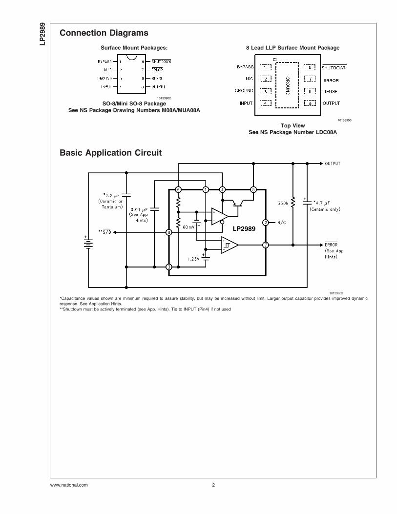
Connection Diagrams
Surface Mount Packages: 8 Lead LLP Surface Mount Package
10133902
SO-8/Mini SO-8 PackageSee NS Package Drawing Numbers M08A/MUA08A
10133950
Top ViewSee NS Package Number LDC08A
Basic Application Circuit
10133903
*Capacitance values shown are minimum required to assure stability, but may be increased without limit. Larger output capacitor provides improved dynamicresponse. See Application Hints.**Shutdown must be actively terminated (see App. Hints). Tie to INPUT (Pin4) if not used
LP29
89
www.national.com 2
Ordering InformationTABLE 1. Package Marking and Ordering Information
Output Voltage Grade Order Information Package Marking Supplied as:
8 Lead LLP
2.5 A LP2989AILD-2.5 L01FA 1000 Units on Tape and Reel
2.5 A LP2989AILDX-2.5 L01FA 4500 Units on Tape and Reel
2.5 STD LP2989ILD-2.5 L01FAB 1000 Units on Tape and Reel
2.5 STD LP2989ILDX-2.5 L01FAB 4500 Units on Tape and Reel
2.8 A LP2989AILD-2.8 L000A 1000 Units on Tape and Reel
2.8 A LP2989AILDX-2.8 L000A 4500 Units on Tape and Reel
2.8 STD LP2989ILD-2.8 L000AB 1000 Units on Tape and Reel
2.8 STD LP2989ILDX-2.8 L000AB 4500 Units on Tape and Reel
2.85 A LP2989AILD-285 L01TA 1000 Units on Tape and Reel
2.85 A LP2989AILDX-285 L01TA 4500 Units on Tape and Reel
2.85 STD LP2989ILD-285 L01TAB 1000 Units on Tape and Reel
2.85 STD LP2989ILDX-285 L01TAB 4500 Units on Tape and Reel
3.0 A LP2989AILD-3.0 L01HA 1000 Units on Tape and Reel
3.0 A LP2989AILDX-3.0 L01HA 4500 Units on Tape and Reel
3.0 STD LP2989ILD-3.0 L01HAB 1000 Units on Tape and Reel
3.0 STD LP2989ILDX-3.0 L01HAB 4500 Units on Tape and Reel
3.3 A LP2989AILD-3.3 L01JA 1000 Units on Tape and Reel
3.3 A LP2989AILDX-3.3 L01JA 4500 Units on Tape and Reel
3.3 STD LP2989ILD-3.3 L01JAB 1000 Units on Tape and Reel
3.3 STD LP2989ILDX-3.3 L01JAB 4500 Units on Tape and Reel
3.6 A LP2989AILD-3.6 L019A 1000 Units on Tape and Reel
3.6 A LP2989AILDX-3.6 L019A 4500 Units on Tape and Reel
3.6 STD LP2989ILD-3.6 L019AB 1000 Units on Tape and Reel
3.6 STD LP2989ILDX-3.6 L019AB 4500 Units on Tape and Reel
4.0 A LP2989AILD-4.0 L01LA 1000 Units on Tape and Reel
4.0 A LP2989AILDX-4.0 L01LA 4500 Units on Tape and Reel
4.0 STD LP2989ILD-4.0 L01LAB 1000 Units on Tape and Reel
4.0 STD LP2989ILDX-4.0 L01LAB 4500 Units on Tape and Reel
5.0 A LP2989AILD-5.0 L01KA 1000 Units on Tape and Reel
5.0 A LP2989AILDX-5.0 L01KA 4500 Units on Tape and Reel
5.0 STD LP2989ILD-5.0 L01KAB 1000 Units on Tape and Reel
5.0 STD LP2989ILDX-5.0 L01KAB 4500 Units on Tape and Reel
8 Lead MSOP (MM)
2.5 A LP2989AIMM-2.5 LA0A 1000 Units on Tape and Reel
2.5 A LP2989AIMMX-2.5 LA0A 3500 Units on Tape and Reel
2.5 STD LP2989IMM-2.5 LA0B 1000 Units on Tape and Reel
2.5 STD LP2989IMMX-2.5 LA0B 3500 Units on Tape and Reel
2.8 A LP2989AIMM-2.8 LA6A 1000 Units on Tape and Reel
2.8 A LP2989AIMMX-2.8 LA6A 3500 Units on Tape and Reel
2.8 STD LP2989IMM-2.8 LA6B 1000 Units on Tape and Reel
2.8 STD LP2989IMMX-2.8 LA6B 3500 Units on Tape and Reel
3.0 A LP2989AIMM-3.0 LA1A 1000 Units on Tape and Reel
3.0 A LP2989AIMMX-3.0 LA1A 3500 Units on Tape and Reel
3.0 STD LP2989IMM-3.0 LA1B 1000 Units on Tape and Reel
3.0 STD LP2989IMMX-3.0 LA1B 3500 Units on Tape and Reel
3.3 A LP2989AIMM-3.3 LA2A 1000 Units on Tape and Reel
3.3 A LP2989AIMMX-3.3 LA2A 3500 Units on Tape and Reel
LP2989
www.national.com3
Ordering Information (Continued)
TABLE 1. Package Marking and Ordering Information (Continued)
Output Voltage Grade Order Information Package Marking Supplied as:
3.3 STD LP2989IMM-3.3 LA2B 1000 Units on Tape and Reel
3.3 STD LP2989IMMX-3.3 LA2B 3500 Units on Tape and Reel
5.0 A LP2989AIMM-5.0 LA4A 1000 Units on Tape and Reel
5.0 A LP2989AIMMX-5.0 LA4A 3500 Units on Tape and Reel
5.0 STD LP2989IMM-5.0 LA4B 1000 Units on Tape and Reel
5.0 STD LP2989IMMX-5.0 LA4B 3500 Units on Tape and Reel
SO-8 (M)
2.5 A LP2989AIMX-2.5 LP2989AIM2.5 2500 Units on Tape and Reel
2.5 A LP2989AIM-2.5 LP2989AIM2.5 Shipped in Anti-Static Rails
2.5 STD LP2989IMX-2.5 LP2989IM2.5 2500 Units on Tape and Reel
2.5 STD LP2989IM-2.5 LP2989IM2.5 Shipped in Anti-Static Rails
3.0 A LP2989AIMX-3.0 LP2989AIM3.0 2500 Units on Tape and Reel
3.0 A LP2989AIM-3.0 LP2989AIM3.0 Shipped in Anti-Static Rails
3.0 STD LP2989IMX-3.0 LP2989IM3.0 2500 Units on Tape and Reel
3.0 STD LP2989IM-3.0 LP2989IM3.0 Shipped in Anti-Static Rails
3.3 A LP2989AIMX-3.3 LP2989AIM3.3 2500 Units on Tape and Reel
3.3 A LP2989AIM-3.3 LP2989AIM3.3 Shipped in Anti-Static Rails
3.3 STD LP2989IMX-3.3 LP2989IM3.3 2500 Units on Tape and Reel
3.3 STD LP2989IM-3.3 LP2989IM3.3 Shipped in Anti-Static Rails
5.0 A LP2989AIMX-5.0 LP2989AIM5.0 2500 Units on Tape and Reel
5.0 A LP2989AIM-5.0 LP2989AIM5.0 Shipped in Anti-Static Rails
5.0 STD LP2989IMX-5.0 LP2989IM5.0 2500 Units on Tape and Reel
5.0 STD LP2989IM-5.0 LP2989IM5.0 Shipped in Anti-Static RailsFor output voltages < 2V, see LP2989LV datasheet.
LP29
89
www.national.com 4
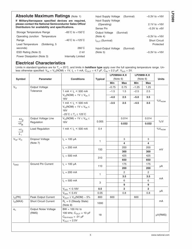
Absolute Maximum Ratings (Note 1)
If Military/Aerospace specified devices are required,please contact the National Semiconductor Sales Office/Distributors for availability and specifications.
Storage Temperature Range −65˚C to +150˚C
Operating Junction TemperatureRange −40˚C to +125˚C
Lead Temperature (Soldering, 5seconds) 260˚C
ESD Rating (Note 2) 2 kV
Power Dissipation (Note 3) Internally Limited
Input Supply Voltage (Survival) −0.3V to +16V
Input Supply Voltage(Operating) 2.1V to +16V
Sense Pin −0.3V to +6V
Output Voltage (Survival)(Note 4) −0.3V to +16V
IOUT (Survival) Short CircuitProtected
Input-Output Voltage (Survival)(Note 5) −0.3V to +16V
Electrical CharacteristicsLimits in standard typeface are for TJ = 25˚C, and limits in boldface type apply over the full operating temperature range. Un-less otherwise specified: VIN = VO(NOM) + 1V, IL = 1 mA, COUT = 4.7 µF, CIN = 2.2 µF, VS/D = 2V.
Symbol Parameter Conditions Typical
LP2989AI-X.X(Note 6)
LP2989I-X.X(Note 6) Units
Min Max Min Max
VO Output VoltageTolerance
−0.75 0.75 −1.25 1.25
%VNOM
1 mA < IL < 500 mAVO(NOM) + 1V ≤ VIN ≤16V
−1.5 1.5 −2.5 2.5
−4.0 2.5 −5.0 3.5
1 mA < IL < 500 mAVO(NOM) + 1V ≤ VIN ≤16V−25˚C ≤ TJ ≤ 125˚C
−3.5 2.5 −4.5 3.5
Output Voltage LineRegulation
VO(NOM) + 1V ≤ VIN ≤16V 0.005
0.014 0.014%/V
0.032 0.032
Load Regulation 1 mA < IL < 500 mA 0.4 %VNOM
VIN–VO Dropout Voltage(Note 7)
IL = 100 µA1
3 3
mV
4 4
IL = 200 mA150
200 200
300 300
IL = 500 mA310
425 425
650 650
IGND Ground Pin Current IL = 100 µA110
175 175µA
200 200
IL = 200 mA1
2 2
mA3.5 3.5
IL = 500 mA3
6 6
9 9
VS/D < 0.18V 0.5 2 2µA
VS/D < 0.4V 0.05 0.8 0.8
IO(PK) Peak Output Current VOUT ≥ VO(NOM) − 5% 800 600 600
mAIO(MAX) Short Circuit Current RL = 0 (Steady State)(Note 9)
1000
en Output Noise Voltage(RMS)
BW = 100 Hz to100 kHz, COUT = 10 µFCBYPASS = .01 µFVOUT = 2.5V
18 µV(RMS)
LP2989
www.national.com5
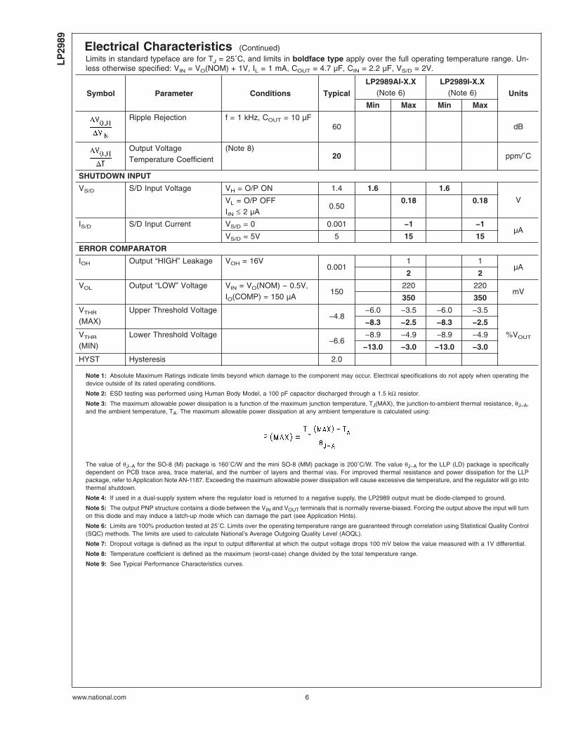
Electrical Characteristics (Continued)Limits in standard typeface are for TJ = 25˚C, and limits in boldface type apply over the full operating temperature range. Un-less otherwise specified: VIN = VO(NOM) + 1V, IL = 1 mA, COUT = 4.7 µF, CIN = 2.2 µF, VS/D = 2V.
Symbol Parameter Conditions Typical
LP2989AI-X.X(Note 6)
LP2989I-X.X(Note 6) Units
Min Max Min Max
Ripple Rejection f = 1 kHz, COUT = 10 µF60 dB
Output VoltageTemperature Coefficient
(Note 8)20 ppm/˚C
SHUTDOWN INPUT
VS/D S/D Input Voltage VH = O/P ON 1.4 1.6 1.6
VVL = O/P OFFIIN ≤ 2 µA
0.500.18 0.18
IS/D S/D Input Current VS/D = 0 0.001 −1 −1µA
VS/D = 5V 5 15 15
ERROR COMPARATOR
IOH Output “HIGH” Leakage VOH = 16V0.001
1 1µA
2 2
VOL Output “LOW” Voltage VIN = VO(NOM) − 0.5V,IO(COMP) = 150 µA
150220 220
mV350 350
VTHR
(MAX)Upper Threshold Voltage
−4.8−6.0 −3.5 −6.0 −3.5
%VOUT
−8.3 −2.5 −8.3 −2.5
VTHR
(MIN)Lower Threshold Voltage
−6.6−8.9 −4.9 −8.9 −4.9
−13.0 −3.0 −13.0 −3.0
HYST Hysteresis 2.0
Note 1: Absolute Maximum Ratings indicate limits beyond which damage to the component may occur. Electrical specifications do not apply when operating thedevice outside of its rated operating conditions.
Note 2: ESD testing was performed using Human Body Model, a 100 pF capacitor discharged through a 1.5 kΩ resistor.
Note 3: The maximum allowable power dissipation is a function of the maximum junction temperature, TJ(MAX), the junction-to-ambient thermal resistance, θJ−A,and the ambient temperature, TA. The maximum allowable power dissipation at any ambient temperature is calculated using:
The value of θJ−A for the SO-8 (M) package is 160˚C/W and the mini SO-8 (MM) package is 200˚C/W. The value θJ−A for the LLP (LD) package is specificallydependent on PCB trace area, trace material, and the number of layers and thermal vias. For improved thermal resistance and power dissipation for the LLPpackage, refer to Application Note AN-1187. Exceeding the maximum allowable power dissipation will cause excessive die temperature, and the regulator will go intothermal shutdown.
Note 4: If used in a dual-supply system where the regulator load is returned to a negative supply, the LP2989 output must be diode-clamped to ground.
Note 5: The output PNP structure contains a diode between the VIN and VOUT terminals that is normally reverse-biased. Forcing the output above the input will turnon this diode and may induce a latch-up mode which can damage the part (see Application Hints).
Note 6: Limits are 100% production tested at 25˚C. Limits over the operating temperature range are guaranteed through correlation using Statistical Quality Control(SQC) methods. The limits are used to calculate National’s Average Outgoing Quality Level (AOQL).
Note 7: Dropout voltage is defined as the input to output differential at which the output voltage drops 100 mV below the value measured with a 1V differential.
Note 8: Temperature coefficient is defined as the maximum (worst-case) change divided by the total temperature range.
Note 9: See Typical Performance Characteristics curves.
LP29
89
www.national.com 6
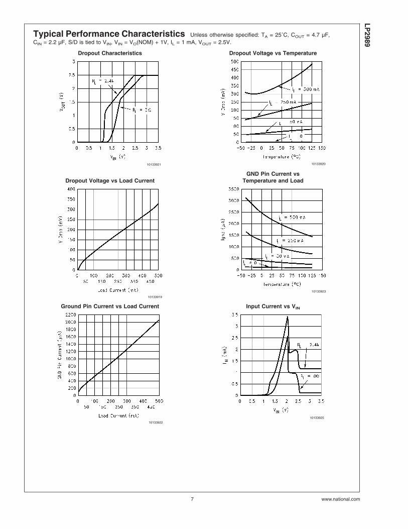
Typical Performance Characteristics Unless otherwise specified: TA = 25˚C, COUT = 4.7 µF,CIN = 2.2 µF, S/D is tied to VIN, VIN = VO(NOM) + 1V, IL = 1 mA, VOUT = 2.5V.
Dropout Characteristics Dropout Voltage vs Temperature
10133921 10133920
Dropout Voltage vs Load CurrentGND Pin Current vs
Temperature and Load
10133919
10133923
Ground Pin Current vs Load Current Input Current vs VIN
10133922
10133925
LP2989
www.national.com7
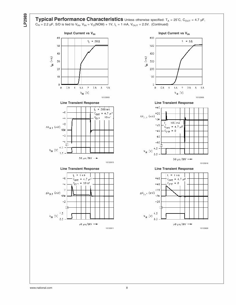
Typical Performance Characteristics Unless otherwise specified: TA = 25˚C, COUT = 4.7 µF,CIN = 2.2 µF, S/D is tied to VIN, VIN = VO(NOM) + 1V, IL = 1 mA, VOUT = 2.5V. (Continued)
Input Current vs VIN Input Current vs VIN
10133905 10133906
Line Transient Response Line Transient Response
10133915 10133916
Line Transient Response Line Transient Response
10133911 10133926
LP29
89
www.national.com 8
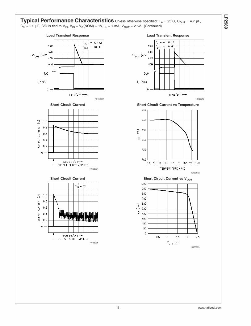
Typical Performance Characteristics Unless otherwise specified: TA = 25˚C, COUT = 4.7 µF,CIN = 2.2 µF, S/D is tied to VIN, VIN = VO(NOM) + 1V, IL = 1 mA, VOUT = 2.5V. (Continued)
Load Transient Response Load Transient Response
10133917 10133918
Short Circuit Current Short Circuit Current vs Temperature
10133934
10133932
Short Circuit Current Short Circuit Current vs VOUT
10133935
10133933
LP2989
www.national.com9
Typical Performance Characteristics Unless otherwise specified: TA = 25˚C, COUT = 4.7 µF,CIN = 2.2 µF, S/D is tied to VIN, VIN = VO(NOM) + 1V, IL = 1 mA, VOUT = 2.5V. (Continued)
Ripple Rejection Ripple Rejection
10133939 10133940
Ripple Rejection Ripple Rejection
10133941 10133942
Ripple Rejection Ripple Rejection
10133943 10133944
LP29
89
www.national.com 10
Typical Performance Characteristics Unless otherwise specified: TA = 25˚C, COUT = 4.7 µF,CIN = 2.2 µF, S/D is tied to VIN, VIN = VO(NOM) + 1V, IL = 1 mA, VOUT = 2.5V. (Continued)
Ripple Rejection Ripple Rejection In Dropout
10133945 10133946
Ripple Rejection vs Load Output Noise Density
10133947
10133936
Output Noise Density Turn-ON Waveform
10133937
10133928
LP2989
www.national.com11
Typical Performance Characteristics Unless otherwise specified: TA = 25˚C, COUT = 4.7 µF,CIN = 2.2 µF, S/D is tied to VIN, VIN = VO(NOM) + 1V, IL = 1 mA, VOUT = 2.5V. (Continued)
Turn-ON Waveform Turn-ON Waveform
10133929 10133930
Turn-ON Waveform IGND vs Shutdown
10133931
10133910
IGND vs Shutdown IGND vs Shutdown
10133908 10133909
LP29
89
www.national.com 12
Typical Performance Characteristics Unless otherwise specified: TA = 25˚C, COUT = 4.7 µF,CIN = 2.2 µF, S/D is tied to VIN, VIN = VO(NOM) + 1V, IL = 1 mA, VOUT = 2.5V. (Continued)
IGND vs Shutdown VOUT vs Shutdown
10133907 10133924
Typical Temperature vs VOUT (LP2989-2.5)
10133955
LP2989
www.national.com13
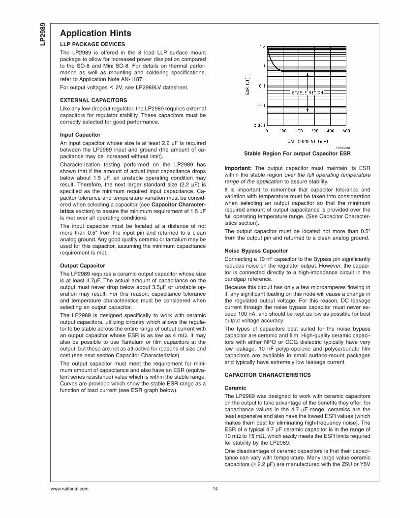
Application HintsLLP PACKAGE DEVICES
The LP2989 is offered in the 8 lead LLP surface mountpackage to allow for increased power dissipation comparedto the SO-8 and Mini SO-8. For details on thermal perfor-mance as well as mounting and soldering specifications,refer to Application Note AN-1187.
For output voltages < 2V, see LP2989LV datasheet.
EXTERNAL CAPACITORS
Like any low-dropout regulator, the LP2989 requires externalcapacitors for regulator stability. These capacitors must becorrectly selected for good performance.
Input Capacitor
An input capacitor whose size is at least 2.2 µF is requiredbetween the LP2989 input and ground (the amount of ca-pacitance may be increased without limit).
Characterization testing performed on the LP2989 hasshown that if the amount of actual input capacitance dropsbelow about 1.5 µF, an unstable operating condition mayresult. Therefore, the next larger standard size (2.2 µF) isspecified as the minimum required input capacitance. Ca-pacitor tolerance and temperature variation must be consid-ered when selecting a capacitor (see Capacitor Character-istics section) to assure the minimum requirement of 1.5 µFis met over all operating conditions.
The input capacitor must be located at a distance of notmore than 0.5" from the input pin and returned to a cleananalog ground. Any good quality ceramic or tantalum may beused for this capacitor, assuming the minimum capacitancerequirement is met.
Output Capacitor
The LP2989 requires a ceramic output capacitor whose sizeis at least 4.7µF. The actual amount of capacitance on theoutput must never drop below about 3.5µF or unstable op-eration may result. For this reason, capacitance toleranceand temperature characteristics must be considered whenselecting an output capacitor.
The LP2989 is designed specifically to work with ceramicoutput capacitors, utilizing circuitry which allows the regula-tor to be stable across the entire range of output current withan output capacitor whose ESR is as low as 4 mΩ. It mayalso be possible to use Tantalum or film capacitors at theoutput, but these are not as attractive for reasons of size andcost (see next section Capacitor Characteristics).
The output capacitor must meet the requirement for mini-mum amount of capacitance and also have an ESR (equiva-lent series resistance) value which is within the stable range.Curves are provided which show the stable ESR range as afunction of load current (see ESR graph below).
10133938
Stable Region For output Capacitor ESR
Important: The output capacitor must maintain its ESRwithin the stable region over the full operating temperaturerange of the application to assure stability.
It is important to remember that capacitor tolerance andvariation with temperature must be taken into considerationwhen selecting an output capacitor so that the minimumrequired amount of output capacitance is provided over thefull operating temperature range. (See Capacitor Character-istics section).
The output capacitor must be located not more than 0.5"from the output pin and returned to a clean analog ground.
Noise Bypass Capacitor
Connecting a 10 nF capacitor to the Bypass pin significantlyreduces noise on the regulator output. However, the capaci-tor is connected directly to a high-impedance circuit in thebandgap reference.
Because this circuit has only a few microamperes flowing init, any significant loading on this node will cause a change inthe regulated output voltage. For this reason, DC leakagecurrent through the noise bypass capacitor must never ex-ceed 100 nA, and should be kept as low as possible for bestoutput voltage accuracy.
The types of capacitors best suited for the noise bypasscapacitor are ceramic and film. High-quality ceramic capaci-tors with either NPO or COG dielectric typically have verylow leakage. 10 nF polypropolene and polycarbonate filmcapacitors are available in small surface-mount packagesand typically have extremely low leakage current.
CAPACITOR CHARACTERISTICS
Ceramic
The LP2989 was designed to work with ceramic capacitorson the output to take advantage of the benefits they offer: forcapacitance values in the 4.7 µF range, ceramics are theleast expensive and also have the lowest ESR values (whichmakes them best for eliminating high-frequency noise). TheESR of a typical 4.7 µF ceramic capacitor is in the range of10 mΩ to 15 mΩ, which easily meets the ESR limits requiredfor stability by the LP2989.
One disadvantage of ceramic capacitors is that their capaci-tance can vary with temperature. Many large value ceramiccapacitors (≥ 2.2 µF) are manufactured with the Z5U or Y5V
LP29
89
www.national.com 14
Application Hints (Continued)
temperature characteristic, which results in the capacitancedropping by more than 50% as the temperature goes from25˚C to 85˚C.
This could cause problems if a 4.7 µF capacitor were usedon the output since it will drop down to approximately 2.4 µFat high ambient temperatures (which could cause theLP2989 to oscillate). Another significant problem with Z5Uand Y5V dielectric devices is that the capacitance dropsseverely with applied voltage. A typical Z5U or Y5V capacitorcan lose 60% of its rated capacitance with half of the ratedvoltage applied to it.
For these reasons, X7R and X5R type ceramic capaci-tors must be used on the input and output of the LP2989
Tantalum
Tantalum capacitors are less desirable than ceramics for useas output capacitors because they are typically more expen-sive when comparing equivalent capacitance and voltageratings in the 1 µF to 4.7 µF range.
Another important consideration is that Tantalum capacitorshave higher ESR values than equivalent size ceramics. Thismeans that while it may be possible to find a Tantalumcapacitor with an ESR value within the stable range, it wouldhave to be larger in capacitance (which means bigger andmore costly) than a ceramic capacitor with the same ESRvalue.
It should also be noted that the ESR of a typical Tantalum willincrease about 2:1 as the temperature goes from 25˚C downto −40˚C, so some guard band must be allowed.
Tantalum capacitors may be used on the input as long as therequirement for minimum capacitance is met.
Film
Polycarbonate and polypropelene film capacitors have ex-cellent electrical performance: their ESR is the lowest of thethree types listed, their capacitance is very stable with tem-perature, and DC leakage current is extremely low.
One disadvantage is that film capacitors are larger in physi-cal size than ceramic or tantalum which makes film a poorchoice for either input or output capacitors.
However, their low leakage makes them a good choice forthe noise bypass capacitor. Since the required amount ofcapacitance is only .01 µF, small surface-mount film capaci-tors are available in this size.
SHUTDOWN INPUT OPERATION
The LP2989 is shut off by driving the Shutdown input low,and turned on by pulling it high. If this feature is not to beused, the Shutdown input should be tied to VIN to keep theregulator output on at all times.
To assure proper operation, the signal source used to drivethe Shutdown input must be able to swing above and belowthe specified turn-on/turn-off voltage thresholds listed in theElectrical Characteristics section under VON/OFF.
To prevent mis-operation, the turn-on (and turn-off) voltagesignals applied to the Shutdown input must have a slew ratewhich is ≥ 40 mV/µs.
CAUTION: the regulator output voltage can not be guaran-teed if a slow-moving AC (or DC) signal is applied that is inthe range between the specified turn-on and turn-off volt-ages listed under the electrical specification VON/OFF (seeElectrical Characteristics).
REVERSE INPUT-OUTPUT VOLTAGE
The PNP power transistor used as the pass element in theLP2989 has an inherent diode connected between the regu-lator output and input.
During normal operation (where the input voltage is higherthan the output) this diode is reverse-biased.
However, if the output is pulled above the input, this diodewill turn ON and current will flow into the regulator output.
In such cases, a parasitic SCR can latch which will allow ahigh current to flow into VIN (and out the ground pin), whichcan damage the part.
In any application where the output may be pulled above theinput, an external Schottky diode must be connected fromVIN to VOUT (cathode on VIN, anode on VOUT), to limit thereverse voltage across the LP2989 to 0.3V (see AbsoluteMaximum Ratings).
LP2989
www.national.com15
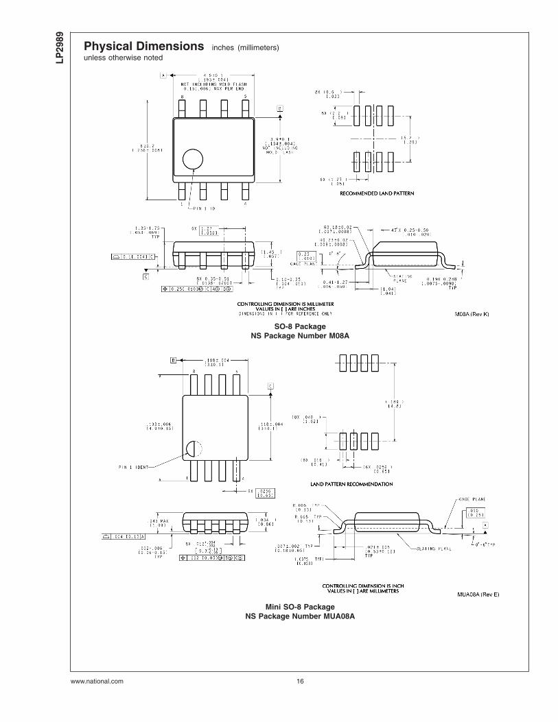
Physical Dimensions inches (millimeters)unless otherwise noted
SO-8 PackageNS Package Number M08A
Mini SO-8 PackageNS Package Number MUA08A
LP29
89
www.national.com 16
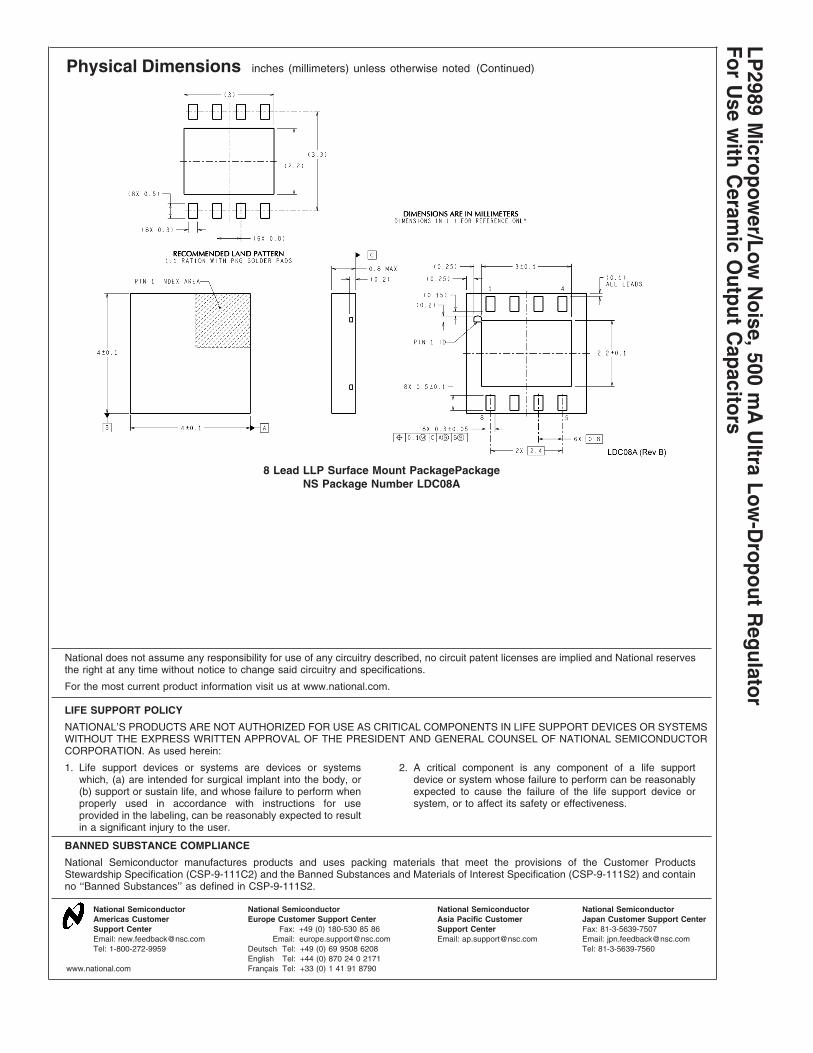
Physical Dimensions inches (millimeters) unless otherwise noted (Continued)
8 Lead LLP Surface Mount PackagePackageNS Package Number LDC08A
National does not assume any responsibility for use of any circuitry described, no circuit patent licenses are implied and National reservesthe right at any time without notice to change said circuitry and specifications.
For the most current product information visit us at www.national.com.
LIFE SUPPORT POLICY
NATIONAL’S PRODUCTS ARE NOT AUTHORIZED FOR USE AS CRITICAL COMPONENTS IN LIFE SUPPORT DEVICES OR SYSTEMSWITHOUT THE EXPRESS WRITTEN APPROVAL OF THE PRESIDENT AND GENERAL COUNSEL OF NATIONAL SEMICONDUCTORCORPORATION. As used herein:
1. Life support devices or systems are devices or systemswhich, (a) are intended for surgical implant into the body, or(b) support or sustain life, and whose failure to perform whenproperly used in accordance with instructions for useprovided in the labeling, can be reasonably expected to resultin a significant injury to the user.
2. A critical component is any component of a life supportdevice or system whose failure to perform can be reasonablyexpected to cause the failure of the life support device orsystem, or to affect its safety or effectiveness.
BANNED SUBSTANCE COMPLIANCE
National Semiconductor manufactures products and uses packing materials that meet the provisions of the Customer ProductsStewardship Specification (CSP-9-111C2) and the Banned Substances and Materials of Interest Specification (CSP-9-111S2) and containno ‘‘Banned Substances’’ as defined in CSP-9-111S2.
National SemiconductorAmericas CustomerSupport CenterEmail: [email protected]: 1-800-272-9959
National SemiconductorEurope Customer Support Center
Fax: +49 (0) 180-530 85 86Email: [email protected]
Deutsch Tel: +49 (0) 69 9508 6208English Tel: +44 (0) 870 24 0 2171Français Tel: +33 (0) 1 41 91 8790
National SemiconductorAsia Pacific CustomerSupport CenterEmail: [email protected]
National SemiconductorJapan Customer Support CenterFax: 81-3-5639-7507Email: [email protected]: 81-3-5639-7560
www.national.com
LP2989
Micropow
er/LowN
oise,500m
AU
ltraLow
-Dropout
Regulator
ForU
sew
ithC
eramic
Output
Capacitors
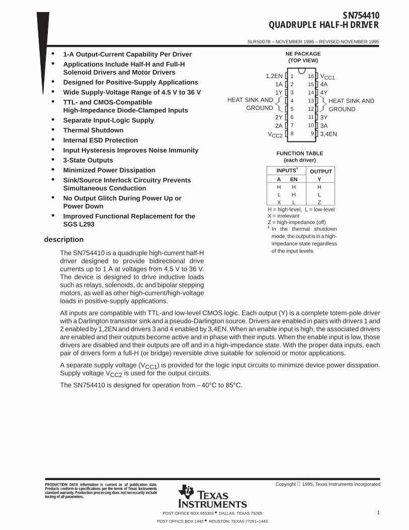
SN754410 QUADRUPLE HALF-H DRIVER
SLRS007B – NOVEMBER 1986 – REVISED NOVEMBER 1995
Copyright 1995, Texas Instruments Incorporated
1POST OFFICE BOX 655303 • DALLAS, TEXAS 75265
POST OFFICE BOX 1443 • HOUSTON, TEXAS 77251–1443
• 1-A Output-Current Capability Per Driver
• Applications Include Half-H and Full-HSolenoid Drivers and Motor Drivers
• Designed for Positive-Supply Applications
• Wide Supply-Voltage Range of 4.5 V to 36 V
• TTL- and CMOS-CompatibleHigh-Impedance Diode-Clamped Inputs
• Separate Input-Logic Supply
• Thermal Shutdown
• Internal ESD Protection
• Input Hysteresis Improves Noise Immunity
• 3-State Outputs
• Minimized Power Dissipation
• Sink/Source Interlock Circuitry PreventsSimultaneous Conduction
• No Output Glitch During Power Up orPower Down
• Improved Functional Replacement for theSGS L293
description
The SN754410 is a quadruple high-current half-Hdriver designed to provide bidirectional drivecurrents up to 1 A at voltages from 4.5 V to 36 V.The device is designed to drive inductive loadssuch as relays, solenoids, dc and bipolar steppingmotors, as well as other high-current/high-voltageloads in positive-supply applications.
All inputs are compatible with TTL-and low-level CMOS logic. Each output (Y) is a complete totem-pole driverwith a Darlington transistor sink and a pseudo-Darlington source. Drivers are enabled in pairs with drivers 1 and2 enabled by 1,2EN and drivers 3 and 4 enabled by 3,4EN. When an enable input is high, the associated driversare enabled and their outputs become active and in phase with their inputs. When the enable input is low, thosedrivers are disabled and their outputs are off and in a high-impedance state. With the proper data inputs, eachpair of drivers form a full-H (or bridge) reversible drive suitable for solenoid or motor applications.
A separate supply voltage (VCC1) is provided for the logic input circuits to minimize device power dissipation.Supply voltage VCC2 is used for the output circuits.
The SN754410 is designed for operation from –40°C to 85°C.
1
2
3
4
5
6
7
8
16
15
14
13
12
11
10
9
1,2EN1A1Y
2Y2A
VCC2
VCC14A4Y HEAT SINK AND GROUND3Y3A3,4EN
HEAT SINK ANDGROUND
AHLX
ENHHL
YHLZ
INPUTS† OUTPUT
FUNCTION TABLE(each driver)
H = high-level, L = low-levelX = irrelevantZ = high-impedance (off)† In the thermal shutdown
mode, the output is in a high-impedance state regardlessof the input levels.
NE PACKAGE(TOP VIEW)
PRODUCTION DATA information is current as of publication date.Products conform to specifications per the terms of Texas Instrumentsstandard warranty. Production processing does not necessarily includetesting of all parameters.
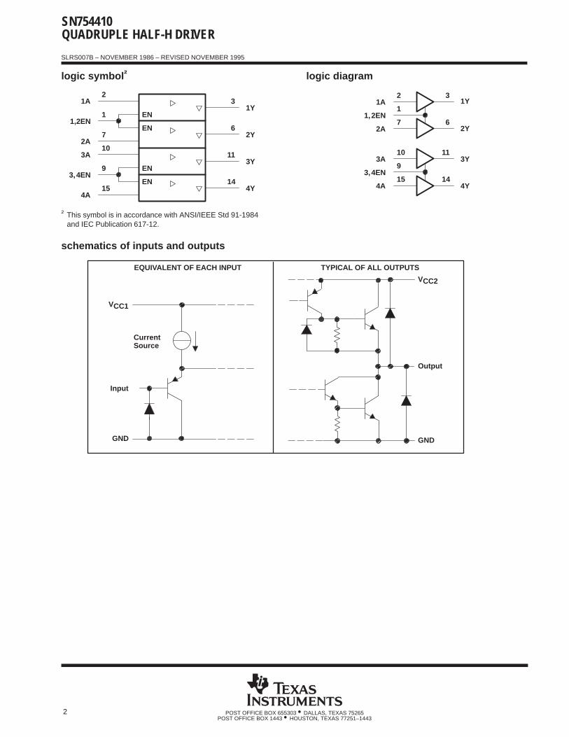
SN754410QUADRUPLE HALF-H DRIVER
SLRS007B – NOVEMBER 1986 – REVISED NOVEMBER 1995
2 POST OFFICE BOX 655303 • DALLAS, TEXAS 75265POST OFFICE BOX 1443 • HOUSTON, TEXAS 77251–1443
logic symbol † logic diagram
EN
EN
EN
EN
4A
3,4EN
3A
2A
1,2EN
1A
15
9
10
7
1
2
4Y
3Y
2Y
1Y
14
11
6
3
4A
3,4EN
3A
2A
1,2EN
1A
15
9
10
7
1
2
4Y
3Y
2Y
1Y
14
11
6
3
† This symbol is in accordance with ANSI/IEEE Std 91-1984and IEC Publication 617-12.
schematics of inputs and outputs
Output
VCC1
EQUIVALENT OF EACH INPUT
CurrentSource
Input
GND
TYPICAL OF ALL OUTPUTS
VCC2
GND
SN754410 QUADRUPLE HALF-H DRIVER
SLRS007B – NOVEMBER 1986 – REVISED NOVEMBER 1995
3POST OFFICE BOX 655303 • DALLAS, TEXAS 75265POST OFFICE BOX 1443 • HOUSTON, TEXAS 77251–1443
absolute maximum ratings over operating free-air temperature range (unless otherwise noted) †
Output supply voltage range, VCC1 (see Note 1) –0.5 V to 36 V. . . . . . . . . . . . . . . . . . . . . . . . . . . . . . . . . . . . . . Output supply voltage range, VCC2 –0.5 V to 36 V. . . . . . . . . . . . . . . . . . . . . . . . . . . . . . . . . . . . . . . . . . . . . . . . . . Input voltage, VI 36 V. . . . . . . . . . . . . . . . . . . . . . . . . . . . . . . . . . . . . . . . . . . . . . . . . . . . . . . . . . . . . . . . . . . . . . . . . . Output voltage range, VO –3 V to VCC2 + 3 V. . . . . . . . . . . . . . . . . . . . . . . . . . . . . . . . . . . . . . . . . . . . . . . . . . . . . Peak output current (nonrepetitive, tw ≤5 ms) ±2 A. . . . . . . . . . . . . . . . . . . . . . . . . . . . . . . . . . . . . . . . . . . . . . . . . Continuous output current, IO ±1.1 A. . . . . . . . . . . . . . . . . . . . . . . . . . . . . . . . . . . . . . . . . . . . . . . . . . . . . . . . . . . . . . Continuous total power dissipation at (or below) 25°C free-air temperature (see Note 2) 2075 mW. . . . . . . . Operating free-air temperature range, TA –40°C to 85°C. . . . . . . . . . . . . . . . . . . . . . . . . . . . . . . . . . . . . . . . . . . . Operating virtual junction temperature range, TJ –40°C to 150°C. . . . . . . . . . . . . . . . . . . . . . . . . . . . . . . . . . . . Storage temperature range, Tstg –65°C to 150°C. . . . . . . . . . . . . . . . . . . . . . . . . . . . . . . . . . . . . . . . . . . . . . . . . . Lead temperature 1,6 mm (1/16 inch) from case for 10 seconds 260°C. . . . . . . . . . . . . . . . . . . . . . . . . . . . . . .
† Stresses beyond those listed under “absolute maximum ratings” may cause permanent damage to the device. These are stress ratings only, andfunctional operation of the device at these or any other conditions beyond those indicated under “recommended operating conditions” is notimplied. Exposure to absolute-maximum-rated conditions for extended periods may affect device reliability.
NOTES: 1. All voltage values are with respect to network GND.2. For operation above 25°C free-air temperature, derate linearly at the rate of 16.6 mW/°C. To avoid exceeding the design maximum
virtual junction temperature, these ratings should not be exceeded. Due to variations in individual device electrical characteristicsand thermal resistance, the built-in thermal overload protection can be activated at power levels slightly above or below the rateddissipation.
recommended operating conditions
MIN MAX UNIT
Output supply voltage, VCC1 4.5 5.5 V
Output supply voltage, VCC2 4.5 36 V
High-level input voltage, VIH 2 5.5 V
Low-level input voltage, VIL –0.3‡ 0.8 V
Operating virtual junction temperature, TJ –40 125 °C
Operating free-air temperature, TA –40 85 °C‡ The algebraic convention, in which the least positive (most negative) limit is designated as minimum, is used in this data sheet for logic voltage
levels.
SN754410QUADRUPLE HALF-H DRIVER
SLRS007B – NOVEMBER 1986 – REVISED NOVEMBER 1995
4 POST OFFICE BOX 655303 • DALLAS, TEXAS 75265POST OFFICE BOX 1443 • HOUSTON, TEXAS 77251–1443
electrical characteristics over recommended ranges of supply voltage and free-air temperature(unless otherwise noted)
PARAMETER TEST CONDITIONS MIN TYP† MAX UNIT
VIK Input clamp voltage II = –12 mA –0.9 –1.5 V
IOH = –0.5 A VCC2–1.5 VCC2–1.1
VOH High-level output voltage IOH = –1 A VCC2–2 V
IOH = –1 A, TJ = 25°C VCC2–1.8 VCC2–1.4
IOL = 0.5 A 1 1.4
VOL Low-level output voltage IOL = 1 A 2 V
IOL = 1 A, TJ = 25°C 1.2 1.8
VO High level output clamp voltageIOK = –0.5 A VCC2+1.4 VCC2+2
VVOKH High-level output clamp voltageIOK = 1 A VCC2+1.9 VCC2+2.5
V
VO Low level output clamp voltageIOK = 0.5 A –1.1 –2
VVOKL Low-level output clamp voltageIOK = –1 A –1.3 –2.5
V
IOZ( ff)Off-state high-impedance-state VO = VCC2 500
µAIOZ(off)g
output current VO = 0 –500µA
IIH High-level input current VI = 5.5 V 10 µA
IIL Low-level input current VI = 0 –10 µA
All outputs at high level 38
ICC1 Output supply current IO = 0 All outputs at low level 70 mA
All outputs at high impedance 25
All outputs at high level 33
ICC2 Output supply current IO = 0 All outputs at low level 20 mA
All outputs at high impedance 5† All typical values are at VCC1 = 5 V, VCC2 = 24 V, TA = 25°C.
switching characteristics, V CC1 = 5 V, VCC2 = 24 V, CL = 30 pF, TA = 25°CPARAMETER TEST CONDITIONS MIN TYP MAX UNIT
td1 Delay time, high-to-low-level output from A input 400 ns
td2 Delay time, low-to-high-level output from A input 800 ns
tTLH Transition time, low-to-high-level output 300 ns
tTHL Transition time, high-to-low-level output See Figure 1 300 ns
tr Rise time, pulse input
tf Fall time, pulse input
tw Pulse duration
ten1 Enable time to the high level 700 ns
ten2 Enable time to the low levelSee Figure 2
400 ns
tdis1 Disable time from the high levelSee Figure 2
900 ns
tdis2 Disable time from the low level 600 ns
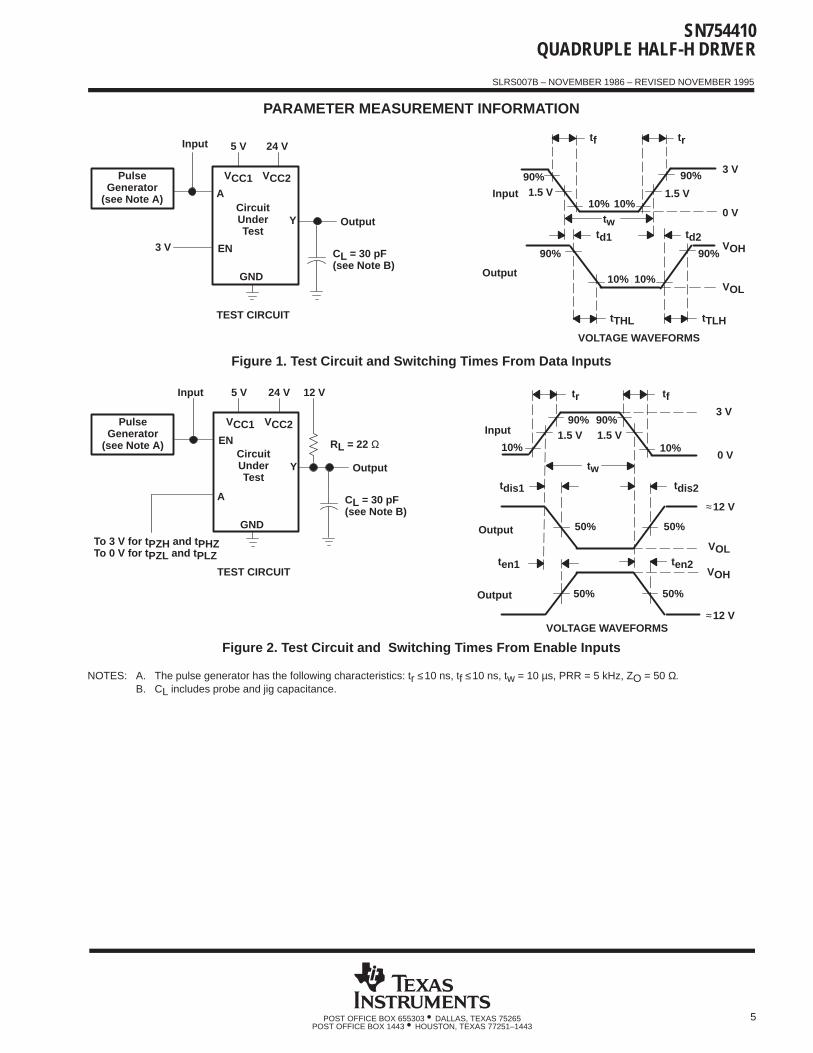
SN754410 QUADRUPLE HALF-H DRIVER
SLRS007B – NOVEMBER 1986 – REVISED NOVEMBER 1995
5POST OFFICE BOX 655303 • DALLAS, TEXAS 75265POST OFFICE BOX 1443 • HOUSTON, TEXAS 77251–1443
PARAMETER MEASUREMENT INFORMATION
PulseGenerator
(see Note A)
VCC1 VCC2
GND
A
EN
CircuitUnderTest
Y
Input 5 V
3 V
24 V
CL = 30 pF(see Note B)
Output
TEST CIRCUIT
90%1.5 V
tf
10%
tr
10%
90%
1.5 V
3 V
0 Vtw
td1 td2VOH
VOL
90% 90%
10% 10%
tTHL tTLH
Input
Output
VOLTAGE WAVEFORMS
Figure 1. Test Circuit and Switching Times From Data Inputs
PulseGenerator
(see Note A)
VCC1 VCC2
GND
A
ENCircuitUnderTest
Y
Input 5 V 24 V
CL = 30 pF(see Note B)
Output
TEST CIRCUIT
To 3 V for t PZH and t PHZTo 0 V for t PZL and t PLZ
12 V
90%1.5 V
tf
10%
tr
10%
90%1.5 V
3 V
0 Vtw
Input
tdis1 tdis2
VOH
VOL
50%Output
VOLTAGE WAVEFORMS
50%
≈12 V
ten1 ten2
50% 50%
≈12 V
Output
RL = 22 Ω
Figure 2. Test Circuit and Switching Times From Enable Inputs
NOTES: A. The pulse generator has the following characteristics: tr ≤10 ns, tf ≤10 ns, tw = 10 µs, PRR = 5 kHz, ZO = 50 Ω.B. CL includes probe and jig capacitance.
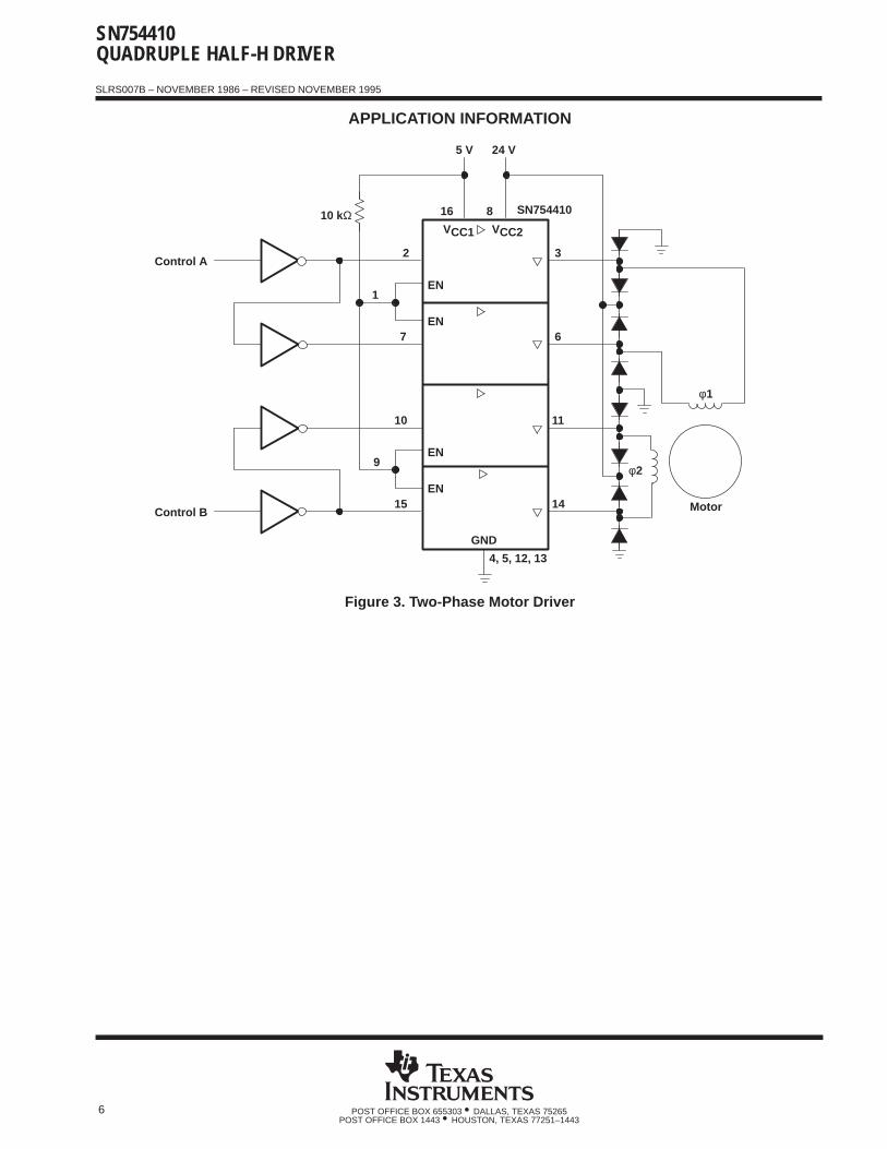
SN754410QUADRUPLE HALF-H DRIVER
SLRS007B – NOVEMBER 1986 – REVISED NOVEMBER 1995
6 POST OFFICE BOX 655303 • DALLAS, TEXAS 75265POST OFFICE BOX 1443 • HOUSTON, TEXAS 77251–1443
APPLICATION INFORMATION
5 V 24 V
SN754410
Control A
10 kΩ 16
Control B
8
2
1
7
10
9
15
4, 5, 12, 13
14
11
6
3
Motor
VCC1
GND
VCC2
φ2
φ1
EN
EN
EN
EN
Figure 3. Two-Phase Motor Driver
PACKAGING INFORMATION
Orderable Device Status (1) PackageType
PackageDrawing
Pins PackageQty
Eco Plan (2) Lead/Ball Finish MSL Peak Temp (3)
SN754410NE ACTIVE PDIP NE 16 25 Pb-Free(RoHS)
CU NIPDAU N / A for Pkg Type
SN754410NEE4 ACTIVE PDIP NE 16 25 Pb-Free(RoHS)
CU NIPDAU N / A for Pkg Type
(1) The marketing status values are defined as follows:ACTIVE: Product device recommended for new designs.LIFEBUY: TI has announced that the device will be discontinued, and a lifetime-buy period is in effect.NRND: Not recommended for new designs. Device is in production to support existing customers, but TI does not recommend using this part ina new design.PREVIEW: Device has been announced but is not in production. Samples may or may not be available.OBSOLETE: TI has discontinued the production of the device.
(2) Eco Plan - The planned eco-friendly classification: Pb-Free (RoHS), Pb-Free (RoHS Exempt), or Green (RoHS & no Sb/Br) - please checkhttp://www.ti.com/productcontent for the latest availability information and additional product content details.TBD: The Pb-Free/Green conversion plan has not been defined.Pb-Free (RoHS): TI's terms "Lead-Free" or "Pb-Free" mean semiconductor products that are compatible with the current RoHS requirementsfor all 6 substances, including the requirement that lead not exceed 0.1% by weight in homogeneous materials. Where designed to be solderedat high temperatures, TI Pb-Free products are suitable for use in specified lead-free processes.Pb-Free (RoHS Exempt): This component has a RoHS exemption for either 1) lead-based flip-chip solder bumps used between the die andpackage, or 2) lead-based die adhesive used between the die and leadframe. The component is otherwise considered Pb-Free (RoHScompatible) as defined above.Green (RoHS & no Sb/Br): TI defines "Green" to mean Pb-Free (RoHS compatible), and free of Bromine (Br) and Antimony (Sb) based flameretardants (Br or Sb do not exceed 0.1% by weight in homogeneous material)
(3) MSL, Peak Temp. -- The Moisture Sensitivity Level rating according to the JEDEC industry standard classifications, and peak soldertemperature.
Important Information and Disclaimer:The information provided on this page represents TI's knowledge and belief as of the date that it isprovided. TI bases its knowledge and belief on information provided by third parties, and makes no representation or warranty as to theaccuracy of such information. Efforts are underway to better integrate information from third parties. TI has taken and continues to takereasonable steps to provide representative and accurate information but may not have conducted destructive testing or chemical analysis onincoming materials and chemicals. TI and TI suppliers consider certain information to be proprietary, and thus CAS numbers and other limitedinformation may not be available for release.
In no event shall TI's liability arising out of such information exceed the total purchase price of the TI part(s) at issue in this document sold by TIto Customer on an annual basis.
PACKAGE OPTION ADDENDUM
www.ti.com 12-Jan-2006
Addendum-Page 1
MECHANICAL DATA
MPDI003 – OCTOBER 1994
1POST OFFICE BOX 655303 • DALLAS, TEXAS 75265
NE (R-PDIP-T**) PLASTIC DUAL-IN-LINE PACKAGE20 PIN SHOWN
2016PINS **
0.780 (19,80)
0.240 (6,10)
0.260 (6,60)
Seating Plane
DIM
0.975 (24,77)
0.914 (23,22)
0.930 (23,62)
1.000 (25,40)
0.260 (6,61)
0.280 (7,11)
Seating Plane
0.010 (0,25) NOM
4040054/B 04/95
0.310 (7,87)0.290 (7,37)
0.070 (1,78) MAX
C
10
0.021 (0,533)0.015 (0,381)
A
11
1
20
0.015 (0,381)0.021 (0,533)
B
0.200 (5,08) MAX
0.020 (0,51) MIN
0.125 (3,17)0.155 (3,94)
0.020 (0,51) MIN
0.200 (5,08) MAX
0.155 (3,94)0.125 (3,17)
M0.010 (0,25)
M0.010 (0,25)0.100 (2,54) 0°–15°
0.100 (2,54)
C
B
A
MIN
MAX
MIN
MAX
MIN
MAX
NOTES: A. All linear dimensions are in inches (millimeters).B. This drawing is subject to change without notice.C. Falls within JEDEC MS-001 (16 pin only)

IMPORTANT NOTICE
Texas Instruments Incorporated and its subsidiaries (TI) reserve the right to make corrections, modifications,enhancements, improvements, and other changes to its products and services at any time and to discontinueany product or service without notice. Customers should obtain the latest relevant information before placingorders and should verify that such information is current and complete. All products are sold subject to TI’s termsand conditions of sale supplied at the time of order acknowledgment.
TI warrants performance of its hardware products to the specifications applicable at the time of sale inaccordance with TI’s standard warranty. Testing and other quality control techniques are used to the extent TIdeems necessary to support this warranty. Except where mandated by government requirements, testing of allparameters of each product is not necessarily performed.
TI assumes no liability for applications assistance or customer product design. Customers are responsible fortheir products and applications using TI components. To minimize the risks associated with customer productsand applications, customers should provide adequate design and operating safeguards.
TI does not warrant or represent that any license, either express or implied, is granted under any TI patent right,copyright, mask work right, or other TI intellectual property right relating to any combination, machine, or processin which TI products or services are used. Information published by TI regarding third-party products or servicesdoes not constitute a license from TI to use such products or services or a warranty or endorsement thereof.Use of such information may require a license from a third party under the patents or other intellectual propertyof the third party, or a license from TI under the patents or other intellectual property of TI.
Reproduction of information in TI data books or data sheets is permissible only if reproduction is withoutalteration and is accompanied by all associated warranties, conditions, limitations, and notices. Reproductionof this information with alteration is an unfair and deceptive business practice. TI is not responsible or liable forsuch altered documentation.
Resale of TI products or services with statements different from or beyond the parameters stated by TI for thatproduct or service voids all express and any implied warranties for the associated TI product or service andis an unfair and deceptive business practice. TI is not responsible or liable for any such statements.
Following are URLs where you can obtain information on other Texas Instruments products and applicationsolutions:
Products Applications
Amplifiers amplifier.ti.com Audio www.ti.com/audio
Data Converters dataconverter.ti.com Automotive www.ti.com/automotive
DSP dsp.ti.com Broadband www.ti.com/broadband
Interface interface.ti.com Digital Control www.ti.com/digitalcontrol
Logic logic.ti.com Military www.ti.com/military
Power Mgmt power.ti.com Optical Networking www.ti.com/opticalnetwork
Microcontrollers microcontroller.ti.com Security www.ti.com/security
Telephony www.ti.com/telephony
Video & Imaging www.ti.com/video
Wireless www.ti.com/wireless
Mailing Address: Texas Instruments
Post Office Box 655303 Dallas, Texas 75265
Copyright 2006, Texas Instruments Incorporated
Archivo: B:\PROYECTO\PROYECTO\integraciontotalv49merina.c 08/05/2008, 12:48:02Archivo: B:\PROYECTO\PROYECTO\integraciontotalv49merina.c 08/05/2008, 12:48:02
/************************************************************************************************* Includes, Exports and External References *************************************************************************************************/#include "mmc2107.h"#include "typedefs.h"#include "mmc2107_initvals.h" /* project hardwaretranslations */
/************************************************************************************************* Macro/Symbol Definitions *************************************************************************************************/#define EnableInterrupts WritePSR(ReadPSR() | IE | EE)#define DisableInterrupts WritePSR(ReadPSR() & ~IE & ~EE)
#define N_MUESTRAS_RADIACION 10 //ojo, que se almacenan en flotantes de 64bits/* Constantes relacionadas con las funciones PIT1 y PIT2 */#define N_MUESTRAS_PERIODO 4
#define OFF_DOZE 1 /* el temporizador es parado en el modo DOZE */#define ON_DOZE 0 /* el temporizador no es parado en el modo DOZE */
/************************************************************************************************* Function Prototypes *************************************************************************************************/int main (void);void Convertidor(void);void LeerTablaDatosConvertidor(void);void BuscarPosicionInicialSol (void);void DetectarPosicionVerticalSol (void);void DetectarPosicionHorizontalSol (void);void MovimientoNormal (void);void CalcularMovimientoHorizontal (void);void CalcularMovimientoVertical (void);double Calcular_Radiacion_Media_Horizontal(INT16U radiacion_actual, INT16Utiempo_radiacion_actual);double Calcular_Radiacion_Media_Vertical(INT16U radiacion_actual_vertical,INT16U tiempo_radiacion_actual_vertical);float Calcular_Media_Periodo1(float dato_tiempo);float Calcular_Media_Periodo2(float dato_tiempo);
void Inicializar_Temporizador1(void);void Inicializar_Temporizador2(void);void Leer_Temporizador1(void);void Leer_Temporizador2(void);
void PIT1(int preescaler,int doze,int enint, int enable,INT16U pmr);
void isr_Queue1_Completion(void);
Página: 1
Archivo: B:\PROYECTO\PROYECTO\integraciontotalv49merina.c 08/05/2008, 12:48:02Archivo: B:\PROYECTO\PROYECTO\integraciontotalv49merina.c 08/05/2008, 12:48:02
void isr_PIT1_PIF(void);//void isr_PIT2_PIF(void);
INT16U myfilter(INT16U input);INT16U myfilter2(INT16U input);INT16U myfilter3(INT16U input);INT16U myfilter4(INT16U input);
/************************************************************************************************* Global Variables *************************************************************************************************/#define UMBRAL_MAXIMO_HORIZONTAL_TENSION 0.085#define UMBRAL_MAXIMO_VERTICAL_TENSION 0.085#define UMBRAL_MINIMO_HORIZONTAL_TENSION 0.085#define UMBRAL_MINIMO_VERTICAL_TENSION 0.085
#define UMBRAL_RADIACION_TENSION 3.44 //umbral para comparar si haynube o no...717
/*#define UMBRAL_MAXIMO_HORIZONTAL 30 //umbral maximo horizontal#define UMBRAL_MAXIMO_VERTICAL 30 //umbral maximo vertical#define UMBRAL_MINIMO_HORIZONTAL 30 //umbral mínimo horizontal#define UMBRAL_MINIMO_VERTICAL 30 //umbral mínimo vertical#define UMBRAL_RADIACION 717 //umbral para comparar si hay nube ono...3.5V*/
#define MEMORIA 4#define MEDIA 4#define REPOSO 0#define HACIA_DERECHA 1#define HACIA_IZQUIERDA 2#define HACIA_ARRIBA 1#define HACIA_ABAJO 2#define BUSCOSOL 0#define NORMAL 1#define NUBE 2
INT16U DatoHorizontalAntesFiltro; //dato horizontal antes delfiltroINT16U DatoVerticalAntesFiltro; //dato vertical antes del filtroINT16U DatoSumadorEjeVerticalAntesFiltro; //dato de suma decorrientes en el eje vertical INT16U DatoSumadorEjeHorizontalAntesFiltro; //dato de suma decorrientes en el eje horizontal
INT16U DatoHorizontalFiltrado; //dato horizontal despues del filtroINT16U DatoVerticalFiltrado; //dato vertical despues del filtroINT16U DatoSumadorEjeHorizontalFiltrado; //dato de suma de corrientes enel eje horizontal despues del filtroINT16U DatoSumadorEjeVerticalFiltrado; //dato de suma de corrientes enel eje vertical despues del filtro
INT16U DatoHorizontal; //dato de toma de decision en el ejehorizontal
Página: 2
Archivo: B:\PROYECTO\PROYECTO\integraciontotalv49merina.c 08/05/2008, 12:48:02Archivo: B:\PROYECTO\PROYECTO\integraciontotalv49merina.c 08/05/2008, 12:48:02
INT16U DatoVertical; //dato de toma de decision en el eje verticalINT16U DatoSumadorEjeHorizontal; //dato de suma de corrientes en eleje horizontalINT16U DatoSumadorEjeVertical; //dato de suma de corrientes en eleje vertical
float cont1; //contador para el periodo en el que se mueve el motorfloat cont2; //contador para el periodo completo de la PWM
float temporizador1; //variable para ir almacenando el valor del contadorque guarda el que se esta moviendo el motorfloat temporizador2; //variable para ir almacenando el periodo completodel PWM
INT16U UMBRAL_RADIACION;INT16U UMBRAL_MAXIMO_HORIZONTAL;INT16U UMBRAL_MAXIMO_VERTICAL;INT16U UMBRAL_MINIMO_HORIZONTAL;INT16U UMBRAL_MINIMO_VERTICAL;
char EstadoEjeVertical; //variables para la maquina de estados del ejeverticalbool Muevete_Arriba;bool Muevete_Abajo;bool ParaEjeVertical;
char EstadoEjeHorizontal; //variables para la maquina de estados del ejehorizontalbool Muevete_Derecha;bool Muevete_Izquierda;bool ParaEjeHorizontal;
bool EncontradoSolEjeVertical; //variables para detectar que ya se haencontrado el sol en el eje vertical y en el eje horizontalbool EncontradoSolEjeHorizontal;
int cuentas;bool nuevodato;
float periodo1; //variable indice de la cola cont1float periodo2; //variable indice de la cola cont1
float media_periodo1;float media_periodo2;
//float datos_periodo1[MEDIA];//float datos_periodo2[MEDIA];//variables radiacion
INT8U inicio; //para recordar que acabamos de empezar a llenar la pila deconversion
/************************************************************************************************* Function Definitions *************************************************************************************************/
Página: 3
Archivo: B:\PROYECTO\PROYECTO\integraciontotalv49merina.c 08/05/2008, 12:48:02Archivo: B:\PROYECTO\PROYECTO\integraciontotalv49merina.c 08/05/2008, 12:48:02
#pragma interrupt on
void isr_PIT1_PIF(void) //rutina de interrupcion paracalcular el tiempo en que se mueve el motorunsigned int temp1;
/*if(temporizador2==0)reg_PORTB.reg=0x01;temporizador2=1;elsereg_PORTB.reg=0x00;temporizador2=0;
/*medido con el oscilocopio esta interrupcion salta cada 72us */
temp1=reg_PCSR1.reg; temp1=temp1|0x0004;reg_PCSR1.reg=temp1;
/*void isr_PIT2_PIF(void) //rutina de interrupcion paracalcular el periodo de la PWMunsigned int temp2;
temporizador2++;
temp2=reg_PCSR2.reg; temp2=temp2|0x0004;reg_PCSR2.reg=temp2;
*/void isr_Queue1_Completion(void) //rutina de interrupcion para leerel convertidorunsigned int temp;signed int m=0,n=0,h=0,f=0;
DatoVerticalAntesFiltro=(INT16U) ((*(volatile INT16U*) (0x00ca0280)));DatoHorizontalAntesFiltro=(INT16U) ((*(volatile INT16U*) (0x00ca0282)));
DatoSumadorEjeVerticalAntesFiltro=(INT16U) ((*(volatile INT16U*)(0x00ca0284)));DatoSumadorEjeHorizontalAntesFiltro=(INT16U) ((*(volatile INT16U*)(0x00ca0286)));
/*
Página: 4
Archivo: B:\PROYECTO\PROYECTO\integraciontotalv49merina.c 08/05/2008, 12:48:02Archivo: B:\PROYECTO\PROYECTO\integraciontotalv49merina.c 08/05/2008, 12:48:02
if(temporizador2==0)reg_PORTB.reg=0x01;temporizador2=1;elsereg_PORTB.reg=0x00;temporizador2=0;
/*medido con el osciloscopio esta interrupcion salta cada 100ms/* limpia bit de interrupcion */ temp=reg_QASR0.reg; temp=temp&0x7fff; reg_QASR0.reg=temp;
temporizador1++;temporizador2++;
cuentas++;nuevodato=TRUE;
#pragma interrupt off
/************************************************************************************************/
/* definiciones de constantes de decisión */
#define NMUESTRAS 5#define VSUMCONLUZV 280 //datos para ecualizar el umbral en funcion de lailuminación-- actualmente no se utilizan #define VSUMCONLUZH 395 //datos para ecualizar el umbral en funcion de lailuminación-- actualmente no se utilizan
//EJE VERTICAL//VALORES DE TENSION
#define V3_0V 614 #define V2_8V 574#define V2_7V 553#define V2_65V 542#define V2_6V 533#define V2_5V 512 /* TENSION 2.5 VOLTIOS EN EL EJE VERTICAL */#define V2_4V 492#define V2_35V 481#define V2_3V 471#define V2_2V 449#define V2_0V 426 #define CALIBL1 0
//EJE HORIZONTAL//VALORES DE TENSION
#define V3_0H 614 #define V2_8H 574#define V2_7H 553
Página: 5
Archivo: B:\PROYECTO\PROYECTO\integraciontotalv49merina.c 08/05/2008, 12:48:02Archivo: B:\PROYECTO\PROYECTO\integraciontotalv49merina.c 08/05/2008, 12:48:02
#define V2_65H 542#define V2_5H 512 /* TENSION 2.5 VOLTIOS EN EL EJE HORIZONTAL */#define V2_35H 481#define V2_3H 471#define V2_2H 449#define V2_0H 426#define CALIBL2 0
/*----------------------------------------------------------------------------------------*//* Filtro digital FIR PASO BAJA DE ORDEN 75, Y CON BANDSTOP EN 0.005 FREC.NYQUIST */
//Definicion de coeficientes
#define b0 1968 #define b1 2014 #define b2 2140 #define b3 2345 #define b4 2629 #define b5 2990 #define b6 3427 #define b7 3937 #define b8 4516 #define b9 5162 #define b10 5870 #define b11 6635 #define b12 7453 #define b13 8317 #define b14 9222 #define b15 10162 #define b16 11131 #define b17 12120 #define b18 13124 #define b19 14135 #define b20 15146 #define b21 16151 #define b22 17141 #define b23 18109 #define b24 19050 #define b25 19955 #define b26 20819 #define b27 21634 #define b28 22396 #define b29 23099 #define b30 23736 #define b31 24305 #define b32 24801 #define b33 25219 #define b34 25558 #define b35 25814 #define b36 25986 #define b37 26072 #define b38 26072 #define b39 25986 #define b40 25814 #define b41 25558 #define b42 25219 #define b43 24801
Página: 6
Archivo: B:\PROYECTO\PROYECTO\integraciontotalv49merina.c 08/05/2008, 12:48:02Archivo: B:\PROYECTO\PROYECTO\integraciontotalv49merina.c 08/05/2008, 12:48:02
#define b44 24305 #define b45 23736 #define b46 23099 #define b47 22396 #define b48 21634 #define b49 20819 #define b50 19955 #define b51 19050 #define b52 18109 #define b53 17141 #define b54 16151 #define b55 15146 #define b56 14135 #define b57 13124 #define b58 12120 #define b59 11131 #define b60 10162 #define b61 9222 #define b62 8317 #define b63 7453 #define b64 6635 #define b65 5870 #define b66 5162 #define b67 4516 #define b68 3937 #define b69 3427 #define b70 2990 #define b71 2629 #define b72 2345 #define b73 2140 #define b74 2014 #define b75 1968
INT32U x[76]; // DEFINICION DE LOS 4 FILTROS QUE SE UTILIZANINT32U x2[76];INT32U x3[76];INT32U x4[76];
INT16U myfilter(INT16U input) //DISEÑO DEL FILTRO... LOS DEMASSON IGUALESINT32U yout=0;INT16U resulta;int i;x[0]=input; yout=b0*x[75] + b1*x[74] + b2*x[73] + b3*x[72] + b4*x[71] + b5*x[70] + b6*x[69] + b7*x[68] + b8*x[67] + b9*x[66] + b10*x[65] + b11*x[64] + b12*x[63]
Página: 7
Archivo: B:\PROYECTO\PROYECTO\integraciontotalv49merina.c 08/05/2008, 12:48:02Archivo: B:\PROYECTO\PROYECTO\integraciontotalv49merina.c 08/05/2008, 12:48:02
+ b13*x[62] + b14*x[61] + b15*x[60] + b16*x[59] + b17*x[58] + b18*x[57] + b19*x[56] + b20*x[55] + b21*x[54] + b22*x[53] + b23*x[52] + b24*x[51] + b25*x[50] + b26*x[49] + b27*x[48] + b28*x[47] + b29*x[46] + b30*x[45] + b31*x[44] + b32*x[43] + b33*x[42] + b34*x[41] + b35*x[40] + b36*x[39] + b37*x[38] + b38*x[37] + b39*x[36] + b40*x[35] + b41*x[34] + b42*x[33] + b43*x[32] + b44*x[31] + b45*x[30] + b46*x[29] + b47*x[28] + b48*x[27] + b49*x[26] + b50*x[25] + b51*x[24] + b52*x[23] + b53*x[22] + b54*x[21] + b55*x[20] + b56*x[19] + b57*x[18] + b58*x[17] + b59*x[16] + b60*x[15] + b61*x[14] + b62*x[13] + b63*x[12] + b64*x[11] + b65*x[10] + b66*x[9] + b67*x[8] + b68*x[7] + b69*x[6] + b70*x[5] + b71*x[4] + b72*x[3]
Página: 8
Archivo: B:\PROYECTO\PROYECTO\integraciontotalv49merina.c 08/05/2008, 12:48:02Archivo: B:\PROYECTO\PROYECTO\integraciontotalv49merina.c 08/05/2008, 12:48:02
+ b73*x[2] + b74*x[1] + b75*x[0] ;
for(i=75;i>0;i--)x[i]=x[i-1];
resulta=yout>>20;return resulta;
INT16U myfilter2(INT16U input)INT32U yout=0;INT16U resulta;int i;x2[0]=input; yout=b0*x2[75] + b1*x2[74] + b2*x2[73] + b3*x2[72] + b4*x2[71] + b5*x2[70] + b6*x2[69] + b7*x2[68] + b8*x2[67] + b9*x2[66] + b10*x2[65] + b11*x2[64] + b12*x2[63] + b13*x2[62] + b14*x2[61] + b15*x2[60] + b16*x2[59] + b17*x2[58] + b18*x2[57] + b19*x2[56] + b20*x2[55] + b21*x2[54] + b22*x2[53] + b23*x2[52] + b24*x2[51] + b25*x2[50] + b26*x2[49] + b27*x2[48] + b28*x2[47] + b29*x2[46] + b30*x2[45] + b31*x2[44] + b32*x2[43] + b33*x2[42] + b34*x2[41] + b35*x2[40] + b36*x2[39] + b37*x2[38] + b38*x2[37] + b39*x2[36] + b40*x2[35] + b41*x2[34]
Página: 9
Archivo: B:\PROYECTO\PROYECTO\integraciontotalv49merina.c 08/05/2008, 12:48:02Archivo: B:\PROYECTO\PROYECTO\integraciontotalv49merina.c 08/05/2008, 12:48:02
+ b42*x2[33] + b43*x2[32] + b44*x2[31] + b45*x2[30] + b46*x2[29] + b47*x2[28] + b48*x2[27] + b49*x2[26] + b50*x2[25] + b51*x2[24] + b52*x2[23] + b53*x2[22] + b54*x2[21] + b55*x2[20] + b56*x2[19] + b57*x2[18] + b58*x2[17] + b59*x2[16] + b60*x2[15] + b61*x2[14] + b62*x2[13] + b63*x2[12] + b64*x2[11] + b65*x2[10] + b66*x2[9] + b67*x2[8] + b68*x2[7] + b69*x2[6] + b70*x2[5] + b71*x2[4] + b72*x2[3] + b73*x2[2] + b74*x2[1] + b75*x2[0];
for(i=75;i>0;i--)x2[i]=x2[i-1]; resulta=yout>>20;return resulta;
INT16U myfilter3(INT16U input)INT32U yout=0;INT16U resulta;int i;x3[0]=input; yout=b0*x3[75] + b1*x3[74] + b2*x3[73] + b3*x3[72] + b4*x3[71] + b5*x3[70] + b6*x3[69] + b7*x3[68] + b8*x3[67] + b9*x3[66]
Página: 10
Archivo: B:\PROYECTO\PROYECTO\integraciontotalv49merina.c 08/05/2008, 12:48:02Archivo: B:\PROYECTO\PROYECTO\integraciontotalv49merina.c 08/05/2008, 12:48:02
+ b10*x3[65] + b11*x3[64] + b12*x3[63] + b13*x3[62] + b14*x3[61] + b15*x3[60] + b16*x3[59] + b17*x3[58] + b18*x3[57] + b19*x3[56] + b20*x3[55] + b21*x3[54] + b22*x3[53] + b23*x3[52] + b24*x3[51] + b25*x3[50] + b26*x3[49] + b27*x3[48] + b28*x3[47] + b29*x3[46] + b30*x3[45] + b31*x3[44] + b32*x3[43] + b33*x3[42] + b34*x3[41] + b35*x3[40] + b36*x3[39] + b37*x3[38] + b38*x3[37] + b39*x3[36] + b40*x3[35] + b41*x3[34] + b42*x3[33] + b43*x3[32] + b44*x3[31] + b45*x3[30] + b46*x3[29] + b47*x3[28] + b48*x3[27] + b49*x3[26] + b50*x3[25] + b51*x3[24] + b52*x3[23] + b53*x3[22] + b54*x3[21] + b55*x3[20] + b56*x3[19] + b57*x3[18] + b58*x3[17] + b59*x3[16] + b60*x3[15] + b61*x3[14] + b62*x3[13] + b63*x3[12] + b64*x3[11] + b65*x3[10] + b66*x3[9] + b67*x3[8] + b68*x3[7] + b69*x3[6]
Página: 11
Archivo: B:\PROYECTO\PROYECTO\integraciontotalv49merina.c 08/05/2008, 12:48:02Archivo: B:\PROYECTO\PROYECTO\integraciontotalv49merina.c 08/05/2008, 12:48:02
+ b70*x3[5] + b71*x3[4] + b72*x3[3] + b73*x3[2] + b74*x3[1] + b75*x3[0];
for(i=75;i>0;i--)x3[i]=x3[i-1]; resulta=yout>>20;return resulta;
INT16U myfilter4(INT16U input)INT32U yout=0;INT16U resulta;int i;x4[0]=input; yout=b0*x4[75] + b1*x4[74] + b2*x4[73] + b3*x4[72] + b4*x4[71] + b5*x4[70] + b6*x4[69] + b7*x4[68] + b8*x4[67] + b9*x4[66] + b10*x4[65] + b11*x4[64] + b12*x4[63] + b13*x4[62] + b14*x4[61] + b15*x4[60] + b16*x4[59] + b17*x4[58] + b18*x4[57] + b19*x4[56] + b20*x4[55] + b21*x4[54] + b22*x4[53] + b23*x4[52] + b24*x4[51] + b25*x4[50] + b26*x4[49] + b27*x4[48] + b28*x4[47] + b29*x4[46] + b30*x4[45] + b31*x4[44] + b32*x4[43] + b33*x4[42] + b34*x4[41] + b35*x4[40] + b36*x4[39] + b37*x4[38]
Página: 12
Archivo: B:\PROYECTO\PROYECTO\integraciontotalv49merina.c 08/05/2008, 12:48:02Archivo: B:\PROYECTO\PROYECTO\integraciontotalv49merina.c 08/05/2008, 12:48:02
+ b38*x4[37] + b39*x4[36] + b40*x4[35] + b41*x4[34] + b42*x4[33] + b43*x4[32] + b44*x4[31] + b45*x4[30] + b46*x4[29] + b47*x4[28] + b48*x4[27] + b49*x4[26] + b50*x4[25] + b51*x4[24] + b52*x4[23] + b53*x4[22] + b54*x4[21] + b55*x4[20] + b56*x4[19] + b57*x4[18] + b58*x4[17] + b59*x4[16] + b60*x4[15] + b61*x4[14] + b62*x4[13] + b63*x4[12] + b64*x4[11] + b65*x4[10] + b66*x4[9] + b67*x4[8] + b68*x4[7] + b69*x4[6] + b70*x4[5] + b71*x4[4] + b72*x4[3] + b73*x4[2] + b74*x4[1] + b75*x4[0] ;
for(i=75;i>0;i--)x4[i]=x4[i-1]; resulta=yout>>20;return resulta;
/************************************************************************************************* Function: int main (void) ** Purpose: Main routine - ** Description: Sigue al sol, en dos ejes, horizontal y vertical. *************************************************************************************************/
int main (void)
Página: 13
Archivo: B:\PROYECTO\PROYECTO\integraciontotalv49merina.c 08/05/2008, 12:48:02Archivo: B:\PROYECTO\PROYECTO\integraciontotalv49merina.c 08/05/2008, 12:48:02
int i=0,j=0,f=0,c=0,d=0;
double radiacion_calculada_horizontal;double radiacion_calculada_vertical;char algoritmo;char modo_manual; // comprueba si estamos en modo manual o no
algoritmo=BUSCOSOL;
radiacion_calculada_horizontal=0; //inicialización de variablesradiacion_calculada_vertical=0; //inicialización de variablescuentas=0;nuevodato=FALSE; //inicialización de variables
EncontradoSolEjeVertical=FALSE; //inicialización de variablesEncontradoSolEjeHorizontal=FALSE; //inicialización de variables
DatoHorizontalAntesFiltro=0; //inicialización de variablesDatoVerticalAntesFiltro=0; //inicialización de variablesDatoHorizontalFiltrado=0; //inicialización de variablesDatoVerticalFiltrado=0; //inicialización de variablesDatoHorizontal=0; //inicialización de variablesDatoVertical=0; //inicialización de variables
DatoSumadorEjeVerticalAntesFiltro=0; //inicialización de variablesDatoSumadorEjeHorizontalAntesFiltro=0; //inicialización de variablesDatoSumadorEjeVerticalFiltrado=0; //inicialización de variablesDatoSumadorEjeHorizontalFiltrado=0; //inicialización de variablesDatoSumadorEjeVertical=0; //inicialización de variablesDatoSumadorEjeHorizontal=0; //inicialización de variables EstadoEjeHorizontal=REPOSO; //EJE HORIZONTAL //inicialización de variablesMuevete_Derecha=FALSE;Muevete_Izquierda=FALSE;ParaEjeHorizontal=FALSE;
EstadoEjeVertical=REPOSO; //EJE VERTICAL //inicialización de variablesMuevete_Abajo=FALSE;Muevete_Arriba=FALSE;ParaEjeVertical=FALSE;
temporizador1=0; //inicialización de variablestemporizador2=0;
cont1=0; //inicialización de variablescont2=0;
periodo1=400; //inicialización de variablesperiodo2=600; //inicialización de variables
for(i=0;i<76;i++) //INICIALIZO LOS FILTROSx[i]=0; for(i=0;i<76;i++)x2[i]=0; for(i=0;i<76;i++)x3[i]=0;
Página: 14
Archivo: B:\PROYECTO\PROYECTO\integraciontotalv49merina.c 08/05/2008, 12:48:02Archivo: B:\PROYECTO\PROYECTO\integraciontotalv49merina.c 08/05/2008, 12:48:02
for(i=0;i<76;i++)x4[i]=0;
media_periodo1=0; //inicialización de variables
media_periodo2=0; //inicialización de variables
i=1;
/*UMBRAL_MAXIMO_HORIZONTAL=(INT16U)(UMBRAL_MAXIMO_HORIZONTAL_TENSION*1024/5);UMBRAL_MAXIMO_VERTICAL=(INT16U)(UMBRAL_MAXIMO_VERTICAL_TENSION*1024/5);UMBRAL_MINIMO_HORIZONTAL=(INT16U)(UMBRAL_MINIMO_HORIZONTAL_TENSION*1024/5);UMBRAL_MINIMO_VERTICAL=(INT16U)(UMBRAL_MINIMO_VERTICAL_TENSION*1024/5);UMBRAL_RADIACION=(INT16U)(UMBRAL_RADIACION_TENSION*1024/5);*/
UMBRAL_MAXIMO_HORIZONTAL=UMBRAL_MAXIMO_HORIZONTAL_TENSION*1024/5;UMBRAL_MAXIMO_VERTICAL=UMBRAL_MAXIMO_VERTICAL_TENSION*1024/5;UMBRAL_MINIMO_HORIZONTAL=UMBRAL_MINIMO_HORIZONTAL_TENSION*1024/5;UMBRAL_MINIMO_VERTICAL=UMBRAL_MINIMO_VERTICAL_TENSION*1024/5;UMBRAL_RADIACION=UMBRAL_RADIACION_TENSION*1024/5;
SystemInit(); /* Initialize all registers of MMC2107 */
Convertidor(); /*configuro el convertidor para que leacada cierto tiempo*/
PIT1(8,ON_DOZE,1,1,5); // habilito interrupcion que mide periodo de la PWM
EnableInterrupts; /* Enable interrupts at the core */
modo_manual=0x00 //inicializo la variable modo manualmodo_manual = reg_PORTB.reg&0x40; //solo me importa pb6 que es donde estael enable
while (cuentas<100) if(nuevodato) LeerTablaDatosConvertidor(); //LEER DATOS ALMACENADOS EN EL CONVERTIDOR nuevodato=FALSE; ; //hasta que se estabilicen los filtros 100 es mayor que 75 el orden del filtro. Espera a que se estabilicen los datos en el filtro
FOREVER // bucle infinito if modo_manual = 0x00 LeerTablaDatosConvertidor(); //LEER DATOS ALMACENADOS EN EL CONVERTIDOR ya esta estabilizado
Página: 15
Archivo: B:\PROYECTO\PROYECTO\integraciontotalv49merina.c 08/05/2008, 12:48:02Archivo: B:\PROYECTO\PROYECTO\integraciontotalv49merina.c 08/05/2008, 12:48:02
radiacion_calculada_horizontal=Calcular_Radiacion_Media_Horizontal( DatoSumadorEjeHorizontal,1); radiacion_calculada_vertical=Calcular_Radiacion_Media_Vertical(Dato SumadorEjeVertical,1); switch(algoritmo) case(BUSCOSOL): reg_PORTB.reg=0x00; //apago led BuscarPosicionInicialSol(); if(EncontradoSolEjeVertical==FALSE||EncontradoSolEjeHorizonta l==FALSE) // sigo aquí mientras no encuentre el sol en los dos ejes algoritmo=BUSCOSOL; else algoritmo=NORMAL; // he encontrado el sol en ambos ejes break; case(NORMAL): CalcularMovimientoVertical(); //ACTUO SOBRE EL MOVIMIENTO VERTICAL CalcularMovimientoHorizontal(); //ACTUO SOBRE EL MOVIMIENTO HORIZONTAL reg_PORTB.reg=0x00; //apago led if (radiacion_calculada_horizontal>=UMBRAL_RADIACION) algoritmo=NUBE; else algoritmo=NORMAL; break; case(NUBE): cuentas=0; while(cuentas<media_periodo1) reg_PORTD.reg=reg_PORTD.reg&0x00 reg_PORTD.reg=reg_PORTD.reg|32; //hace algo con el puerto D, para mover motores.
Página: 16
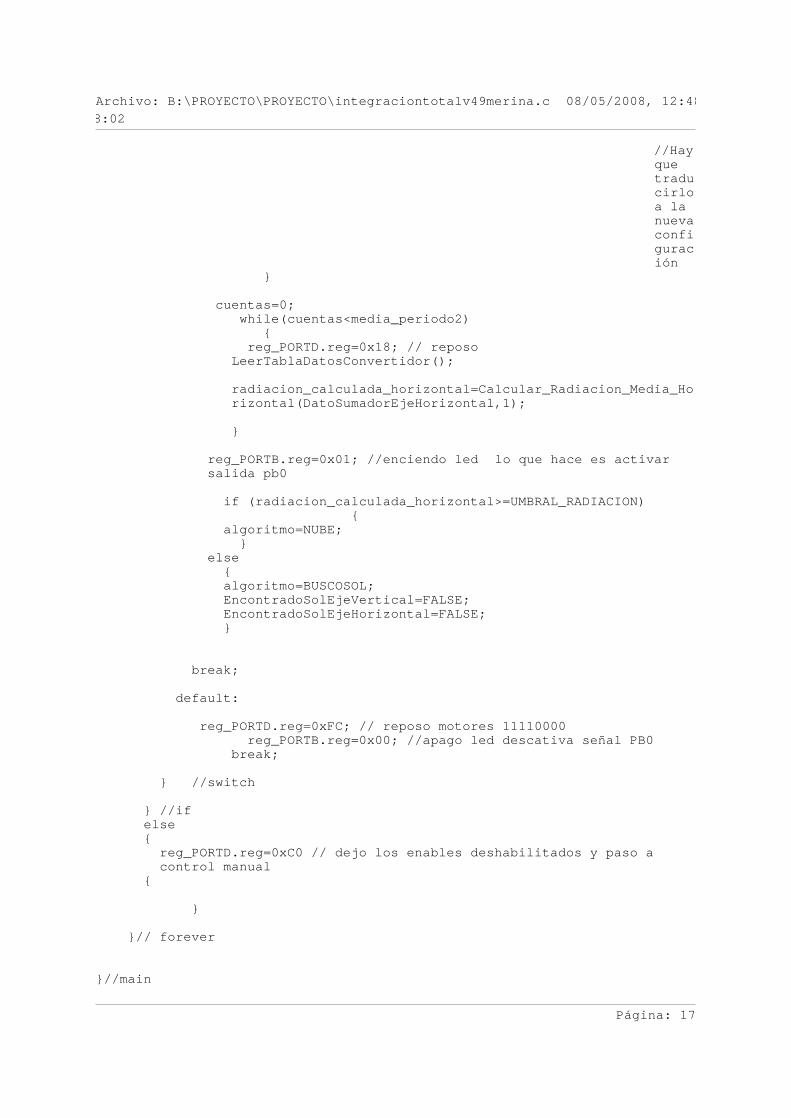
Archivo: B:\PROYECTO\PROYECTO\integraciontotalv49merina.c 08/05/2008, 12:48:02Archivo: B:\PROYECTO\PROYECTO\integraciontotalv49merina.c 08/05/2008, 12:48:02
//Hay que tradu cirlo a la nueva confi gurac ión cuentas=0; while(cuentas<media_periodo2) reg_PORTD.reg=0x18; // reposo LeerTablaDatosConvertidor(); radiacion_calculada_horizontal=Calcular_Radiacion_Media_Ho rizontal(DatoSumadorEjeHorizontal,1); reg_PORTB.reg=0x01; //enciendo led lo que hace es activar salida pb0 if (radiacion_calculada_horizontal>=UMBRAL_RADIACION) algoritmo=NUBE; else algoritmo=BUSCOSOL; EncontradoSolEjeVertical=FALSE; EncontradoSolEjeHorizontal=FALSE; break; default: reg_PORTD.reg=0xFC; // reposo motores 11110000 reg_PORTB.reg=0x00; //apago led descativa señal PB0 break; //switch
//if else reg_PORTD.reg=0xC0 // dejo los enables deshabilitados y paso a control manual // forever
//main
Página: 17
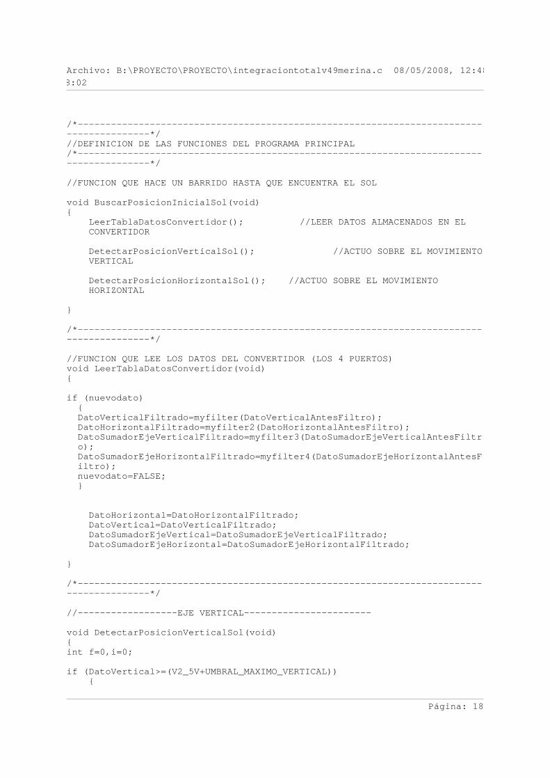
Archivo: B:\PROYECTO\PROYECTO\integraciontotalv49merina.c 08/05/2008, 12:48:02Archivo: B:\PROYECTO\PROYECTO\integraciontotalv49merina.c 08/05/2008, 12:48:02
/*----------------------------------------------------------------------------------------*///DEFINICION DE LAS FUNCIONES DEL PROGRAMA PRINCIPAL/*----------------------------------------------------------------------------------------*/
//FUNCION QUE HACE UN BARRIDO HASTA QUE ENCUENTRA EL SOL
void BuscarPosicionInicialSol(void) LeerTablaDatosConvertidor(); //LEER DATOS ALMACENADOS EN EL CONVERTIDOR DetectarPosicionVerticalSol(); //ACTUO SOBRE EL MOVIMIENTO VERTICAL DetectarPosicionHorizontalSol(); //ACTUO SOBRE EL MOVIMIENTO HORIZONTAL
/*----------------------------------------------------------------------------------------*/
//FUNCION QUE LEE LOS DATOS DEL CONVERTIDOR (LOS 4 PUERTOS)void LeerTablaDatosConvertidor(void)
if (nuevodato) DatoVerticalFiltrado=myfilter(DatoVerticalAntesFiltro); DatoHorizontalFiltrado=myfilter2(DatoHorizontalAntesFiltro); DatoSumadorEjeVerticalFiltrado=myfilter3(DatoSumadorEjeVerticalAntesFiltr o); DatoSumadorEjeHorizontalFiltrado=myfilter4(DatoSumadorEjeHorizontalAntesF iltro); nuevodato=FALSE; DatoHorizontal=DatoHorizontalFiltrado; DatoVertical=DatoVerticalFiltrado; DatoSumadorEjeVertical=DatoSumadorEjeVerticalFiltrado; DatoSumadorEjeHorizontal=DatoSumadorEjeHorizontalFiltrado;
/*----------------------------------------------------------------------------------------*/
//------------------EJE VERTICAL-----------------------
void DetectarPosicionVerticalSol(void)int f=0,i=0;
if (DatoVertical>=(V2_5V+UMBRAL_MAXIMO_VERTICAL))
Página: 18
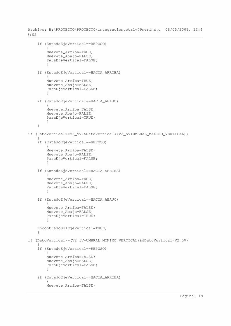
Archivo: B:\PROYECTO\PROYECTO\integraciontotalv49merina.c 08/05/2008, 12:48:02Archivo: B:\PROYECTO\PROYECTO\integraciontotalv49merina.c 08/05/2008, 12:48:02
if (EstadoEjeVertical==REPOSO) Muevete_Arriba=TRUE; Muevete_Abajo=FALSE; ParaEjeVertical=FALSE; if (EstadoEjeVertical==HACIA_ARRIBA) Muevete_Arriba=TRUE; Muevete_Abajo=FALSE; ParaEjeVertical=FALSE; if (EstadoEjeVertical==HACIA_ABAJO) Muevete_Arriba=FALSE; Muevete_Abajo=FALSE; ParaEjeVertical=TRUE; if (DatoVertical>=V2_5V&&DatoVertical<(V2_5V+UMBRAL_MAXIMO_VERTICAL)) if (EstadoEjeVertical==REPOSO) Muevete_Arriba=FALSE; Muevete_Abajo=FALSE; ParaEjeVertical=FALSE; if (EstadoEjeVertical==HACIA_ARRIBA) Muevete_Arriba=TRUE; Muevete_Abajo=FALSE; ParaEjeVertical=FALSE; if (EstadoEjeVertical==HACIA_ABAJO) Muevete_Arriba=FALSE; Muevete_Abajo=FALSE; ParaEjeVertical=TRUE; EncontradoSolEjeVertical=TRUE;
if (DatoVertical>=(V2_5V-UMBRAL_MINIMO_VERTICAL)&&DatoVertical<V2_5V) if (EstadoEjeVertical==REPOSO) Muevete_Arriba=FALSE; Muevete_Abajo=FALSE; ParaEjeVertical=FALSE; if (EstadoEjeVertical==HACIA_ARRIBA) Muevete_Arriba=FALSE;
Página: 19
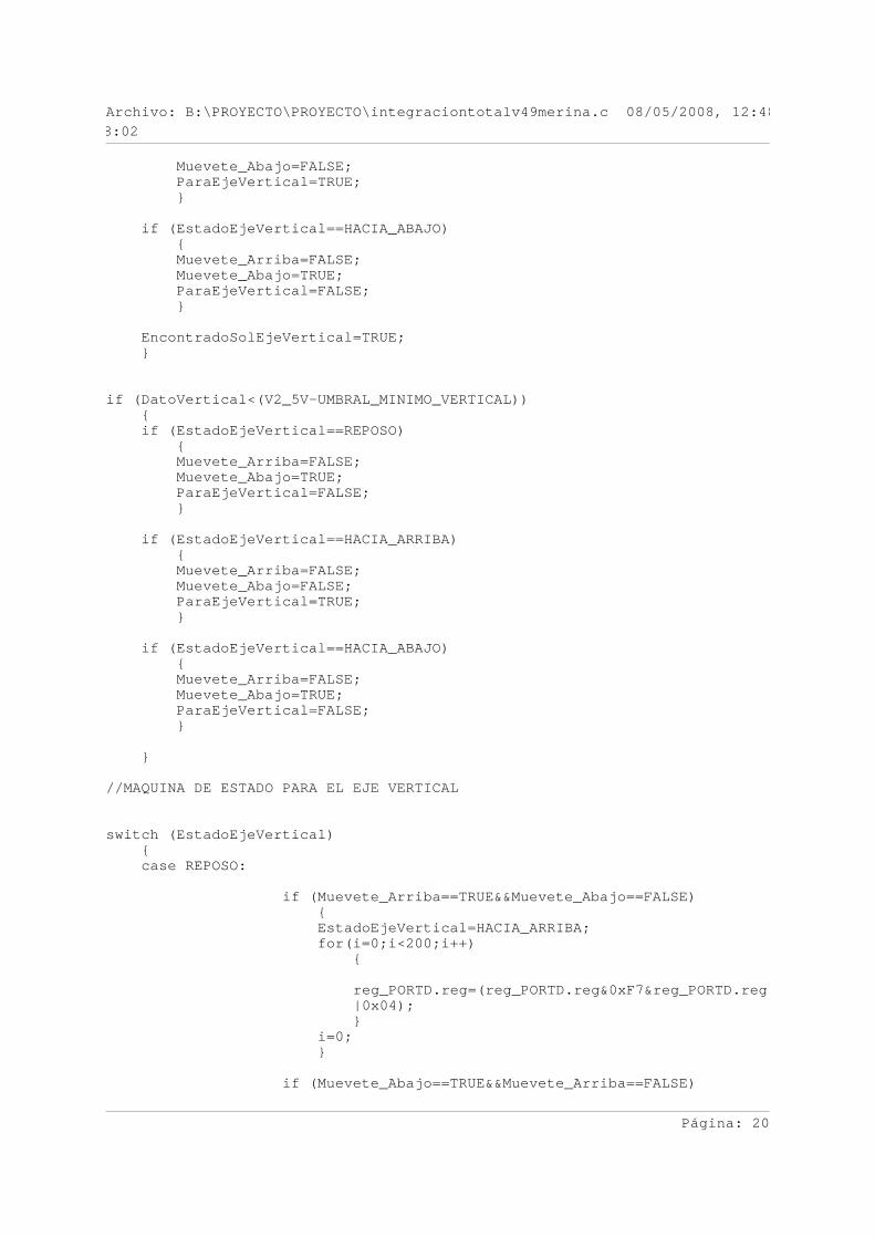
Archivo: B:\PROYECTO\PROYECTO\integraciontotalv49merina.c 08/05/2008, 12:48:02Archivo: B:\PROYECTO\PROYECTO\integraciontotalv49merina.c 08/05/2008, 12:48:02
Muevete_Abajo=FALSE; ParaEjeVertical=TRUE; if (EstadoEjeVertical==HACIA_ABAJO) Muevete_Arriba=FALSE; Muevete_Abajo=TRUE; ParaEjeVertical=FALSE; EncontradoSolEjeVertical=TRUE;
if (DatoVertical<(V2_5V-UMBRAL_MINIMO_VERTICAL)) if (EstadoEjeVertical==REPOSO) Muevete_Arriba=FALSE; Muevete_Abajo=TRUE; ParaEjeVertical=FALSE; if (EstadoEjeVertical==HACIA_ARRIBA) Muevete_Arriba=FALSE; Muevete_Abajo=FALSE; ParaEjeVertical=TRUE; if (EstadoEjeVertical==HACIA_ABAJO) Muevete_Arriba=FALSE; Muevete_Abajo=TRUE; ParaEjeVertical=FALSE; //MAQUINA DE ESTADO PARA EL EJE VERTICAL
switch (EstadoEjeVertical) case REPOSO:
if (Muevete_Arriba==TRUE&&Muevete_Abajo==FALSE) EstadoEjeVertical=HACIA_ARRIBA; for(i=0;i<200;i++) reg_PORTD.reg=(reg_PORTD.reg&0xF7®_PORTD.reg |0x04); i=0;
if (Muevete_Abajo==TRUE&&Muevete_Arriba==FALSE)
Página: 20
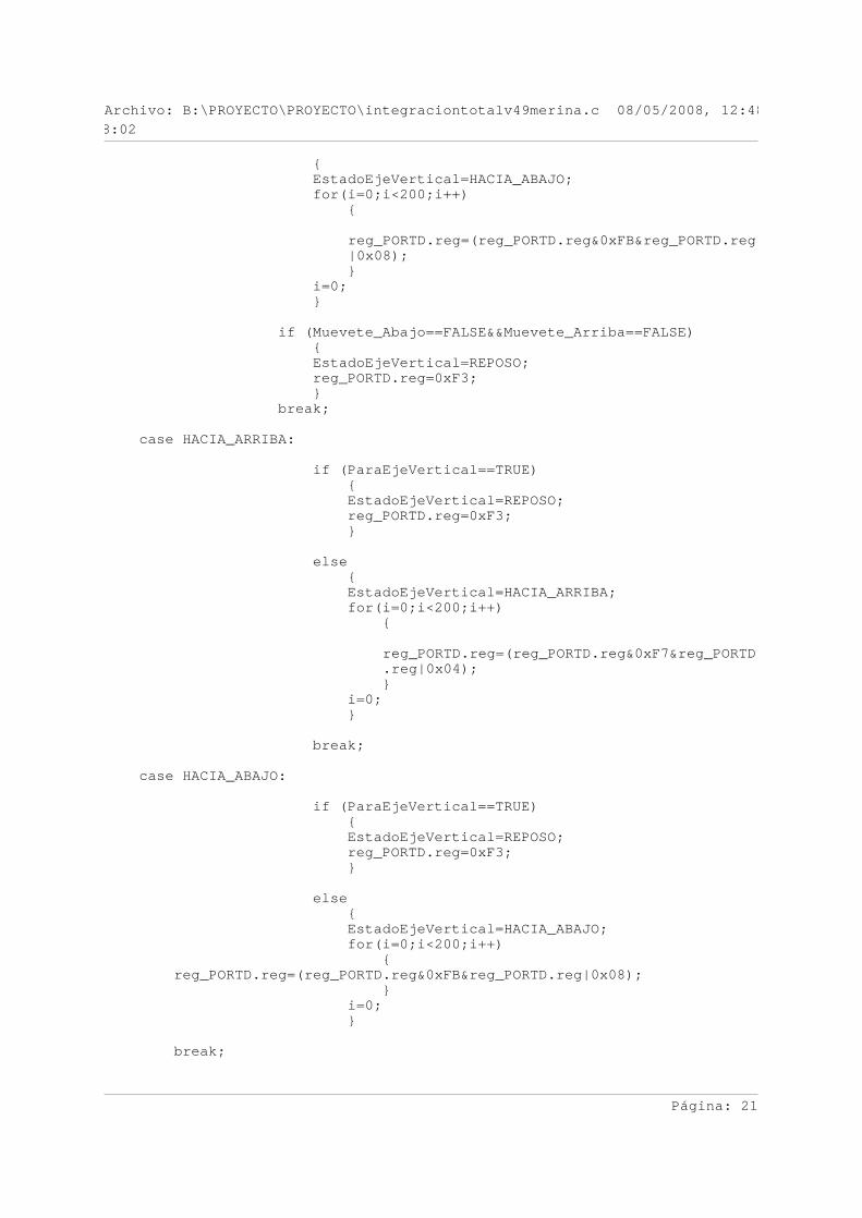
Archivo: B:\PROYECTO\PROYECTO\integraciontotalv49merina.c 08/05/2008, 12:48:02Archivo: B:\PROYECTO\PROYECTO\integraciontotalv49merina.c 08/05/2008, 12:48:02
EstadoEjeVertical=HACIA_ABAJO; for(i=0;i<200;i++) reg_PORTD.reg=(reg_PORTD.reg&0xFB®_PORTD.reg |0x08); i=0;
if (Muevete_Abajo==FALSE&&Muevete_Arriba==FALSE) EstadoEjeVertical=REPOSO; reg_PORTD.reg=0xF3; break; case HACIA_ARRIBA: if (ParaEjeVertical==TRUE) EstadoEjeVertical=REPOSO; reg_PORTD.reg=0xF3;
else EstadoEjeVertical=HACIA_ARRIBA; for(i=0;i<200;i++) reg_PORTD.reg=(reg_PORTD.reg&0xF7®_PORTD .reg|0x04); i=0; break;
case HACIA_ABAJO:
if (ParaEjeVertical==TRUE) EstadoEjeVertical=REPOSO; reg_PORTD.reg=0xF3;
else EstadoEjeVertical=HACIA_ABAJO; for(i=0;i<200;i++) reg_PORTD.reg=(reg_PORTD.reg&0xFB®_PORTD.reg|0x08); i=0; break;
Página: 21
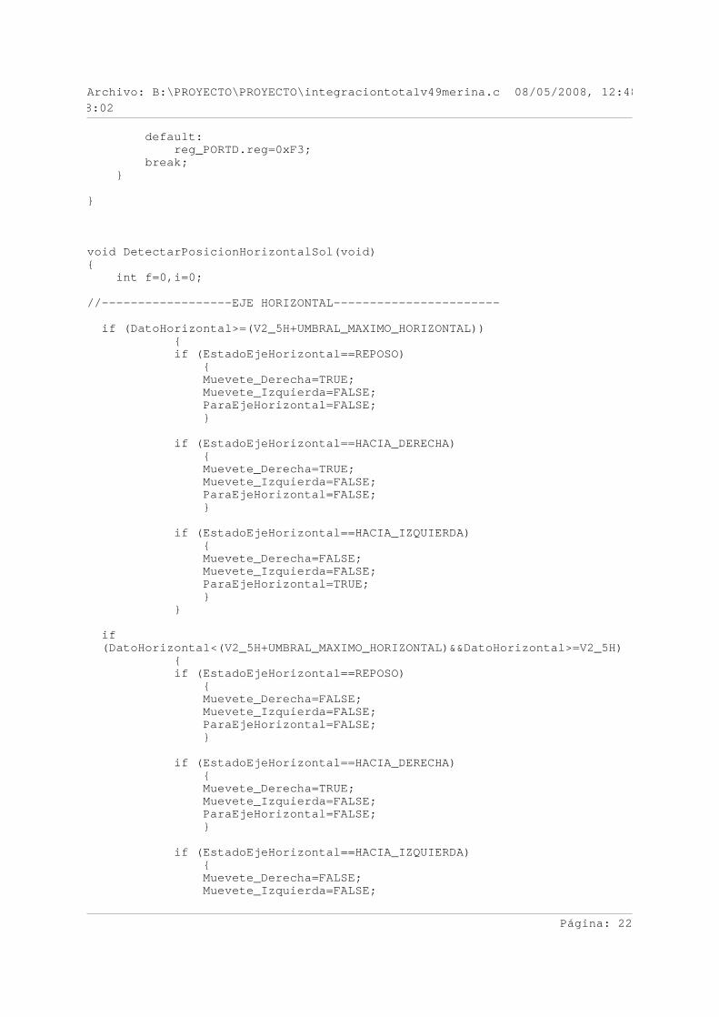
Archivo: B:\PROYECTO\PROYECTO\integraciontotalv49merina.c 08/05/2008, 12:48:02Archivo: B:\PROYECTO\PROYECTO\integraciontotalv49merina.c 08/05/2008, 12:48:02
default: reg_PORTD.reg=0xF3; break;
void DetectarPosicionHorizontalSol(void) int f=0,i=0;
//------------------EJE HORIZONTAL-----------------------
if (DatoHorizontal>=(V2_5H+UMBRAL_MAXIMO_HORIZONTAL)) if (EstadoEjeHorizontal==REPOSO) Muevete_Derecha=TRUE; Muevete_Izquierda=FALSE; ParaEjeHorizontal=FALSE; if (EstadoEjeHorizontal==HACIA_DERECHA) Muevete_Derecha=TRUE; Muevete_Izquierda=FALSE; ParaEjeHorizontal=FALSE; if (EstadoEjeHorizontal==HACIA_IZQUIERDA) Muevete_Derecha=FALSE; Muevete_Izquierda=FALSE; ParaEjeHorizontal=TRUE;
if (DatoHorizontal<(V2_5H+UMBRAL_MAXIMO_HORIZONTAL)&&DatoHorizontal>=V2_5H) if (EstadoEjeHorizontal==REPOSO) Muevete_Derecha=FALSE; Muevete_Izquierda=FALSE; ParaEjeHorizontal=FALSE; if (EstadoEjeHorizontal==HACIA_DERECHA) Muevete_Derecha=TRUE; Muevete_Izquierda=FALSE; ParaEjeHorizontal=FALSE; if (EstadoEjeHorizontal==HACIA_IZQUIERDA) Muevete_Derecha=FALSE; Muevete_Izquierda=FALSE;
Página: 22
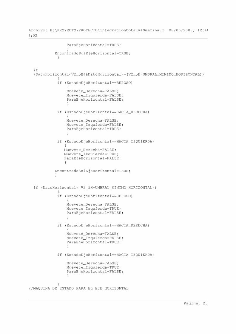
Archivo: B:\PROYECTO\PROYECTO\integraciontotalv49merina.c 08/05/2008, 12:48:02Archivo: B:\PROYECTO\PROYECTO\integraciontotalv49merina.c 08/05/2008, 12:48:02
ParaEjeHorizontal=TRUE; EncontradoSolEjeHorizontal=TRUE; if (DatoHorizontal<V2_5H&&DatoHorizontal>=(V2_5H-UMBRAL_MINIMO_HORIZONTAL)) if (EstadoEjeHorizontal==REPOSO) Muevete_Derecha=FALSE; Muevete_Izquierda=FALSE; ParaEjeHorizontal=FALSE; if (EstadoEjeHorizontal==HACIA_DERECHA) Muevete_Derecha=FALSE; Muevete_Izquierda=FALSE; ParaEjeHorizontal=TRUE; if (EstadoEjeHorizontal==HACIA_IZQUIERDA) Muevete_Derecha=FALSE; Muevete_Izquierda=TRUE; ParaEjeHorizontal=FALSE; EncontradoSolEjeHorizontal=TRUE;
if (DatoHorizontal<(V2_5H-UMBRAL_MINIMO_HORIZONTAL)) if (EstadoEjeHorizontal==REPOSO) Muevete_Derecha=FALSE; Muevete_Izquierda=TRUE; ParaEjeHorizontal=FALSE; if (EstadoEjeHorizontal==HACIA_DERECHA) Muevete_Derecha=FALSE; Muevete_Izquierda=FALSE; ParaEjeHorizontal=TRUE; if (EstadoEjeHorizontal==HACIA_IZQUIERDA) Muevete_Derecha=FALSE; Muevete_Izquierda=TRUE; ParaEjeHorizontal=FALSE; //MAQUINA DE ESTADO PARA EL EJE HORIZONTAL
Página: 23
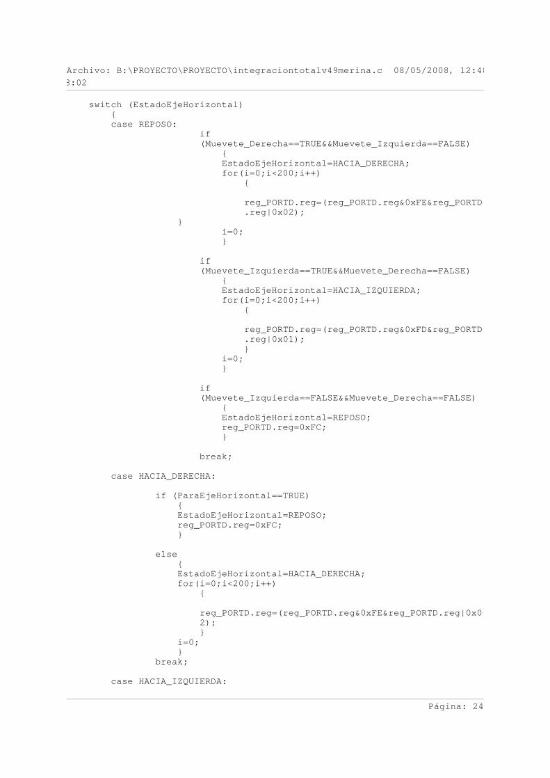
Archivo: B:\PROYECTO\PROYECTO\integraciontotalv49merina.c 08/05/2008, 12:48:02Archivo: B:\PROYECTO\PROYECTO\integraciontotalv49merina.c 08/05/2008, 12:48:02
switch (EstadoEjeHorizontal) case REPOSO: if (Muevete_Derecha==TRUE&&Muevete_Izquierda==FALSE) EstadoEjeHorizontal=HACIA_DERECHA; for(i=0;i<200;i++) reg_PORTD.reg=(reg_PORTD.reg&0xFE®_PORTD .reg|0x02); i=0;
if (Muevete_Izquierda==TRUE&&Muevete_Derecha==FALSE) EstadoEjeHorizontal=HACIA_IZQUIERDA; for(i=0;i<200;i++) reg_PORTD.reg=(reg_PORTD.reg&0xFD®_PORTD .reg|0x01); i=0;
if (Muevete_Izquierda==FALSE&&Muevete_Derecha==FALSE) EstadoEjeHorizontal=REPOSO; reg_PORTD.reg=0xFC; break; case HACIA_DERECHA: if (ParaEjeHorizontal==TRUE) EstadoEjeHorizontal=REPOSO; reg_PORTD.reg=0xFC;
else EstadoEjeHorizontal=HACIA_DERECHA; for(i=0;i<200;i++) reg_PORTD.reg=(reg_PORTD.reg&0xFE®_PORTD.reg|0x0 2); i=0; break;
case HACIA_IZQUIERDA:
Página: 24

Archivo: B:\PROYECTO\PROYECTO\integraciontotalv49merina.c 08/05/2008, 12:48:02Archivo: B:\PROYECTO\PROYECTO\integraciontotalv49merina.c 08/05/2008, 12:48:02
if (ParaEjeHorizontal==TRUE) EstadoEjeHorizontal=REPOSO; reg_PORTD.reg=0xFC;
else EstadoEjeHorizontal=HACIA_IZQUIERDA; for(i=0;i<200;i++) reg_PORTD.reg=(reg_PORTD.reg&0xFD®_PORTD.reg|0x0 1); i=0; break;
default: reg_PORTD.reg=0xFC; break;
//FUNCION QUE ELIGE ENTRE ALGORITMO DE NUBE Y FUNCIONAMIENTO NORMALvoid MovimientoNormal(void)
//------------------MOVIMIENTO EJE VERTICAL-----------------------void CalcularMovimientoVertical(void)if (DatoVertical>=(V2_5V+UMBRAL_MAXIMO_VERTICAL)) if (EstadoEjeVertical==REPOSO) Muevete_Arriba=TRUE; Muevete_Abajo=FALSE; ParaEjeVertical=FALSE; if (EstadoEjeVertical==HACIA_ARRIBA) Muevete_Arriba=TRUE; Muevete_Abajo=FALSE; ParaEjeVertical=FALSE;
Página: 25
Archivo: B:\PROYECTO\PROYECTO\integraciontotalv49merina.c 08/05/2008, 12:48:02Archivo: B:\PROYECTO\PROYECTO\integraciontotalv49merina.c 08/05/2008, 12:48:02
if (EstadoEjeVertical==HACIA_ABAJO) Muevete_Arriba=FALSE; Muevete_Abajo=FALSE; ParaEjeVertical=TRUE; if (DatoVertical>=V2_5V&&DatoVertical<(V2_5V+UMBRAL_MAXIMO_VERTICAL)) if (EstadoEjeVertical==REPOSO) Muevete_Arriba=FALSE; Muevete_Abajo=FALSE; ParaEjeVertical=FALSE; if (EstadoEjeVertical==HACIA_ARRIBA) Muevete_Arriba=TRUE; Muevete_Abajo=FALSE; ParaEjeVertical=FALSE; if (EstadoEjeVertical==HACIA_ABAJO) Muevete_Arriba=FALSE; Muevete_Abajo=FALSE; ParaEjeVertical=TRUE;
if (DatoVertical>=(V2_5V-UMBRAL_MINIMO_VERTICAL)&&DatoVertical<V2_5V) if (EstadoEjeVertical==REPOSO) Muevete_Arriba=FALSE; Muevete_Abajo=FALSE; ParaEjeVertical=FALSE; if (EstadoEjeVertical==HACIA_ARRIBA) Muevete_Arriba=FALSE; Muevete_Abajo=FALSE; ParaEjeVertical=TRUE; if (EstadoEjeVertical==HACIA_ABAJO) Muevete_Arriba=FALSE; Muevete_Abajo=TRUE; ParaEjeVertical=FALSE;
if (DatoVertical<(V2_5V-UMBRAL_MINIMO_VERTICAL)) if (EstadoEjeVertical==REPOSO) Muevete_Arriba=FALSE; Muevete_Abajo=TRUE; ParaEjeVertical=FALSE;
Página: 26
Archivo: B:\PROYECTO\PROYECTO\integraciontotalv49merina.c 08/05/2008, 12:48:02Archivo: B:\PROYECTO\PROYECTO\integraciontotalv49merina.c 08/05/2008, 12:48:02
if (EstadoEjeVertical==HACIA_ARRIBA) Muevete_Arriba=FALSE; Muevete_Abajo=FALSE; ParaEjeVertical=TRUE; if (EstadoEjeVertical==HACIA_ABAJO) Muevete_Arriba=FALSE; Muevete_Abajo=TRUE; ParaEjeVertical=FALSE; //MAQUINA DE ESTADO PARA EL EJE VERTICAL
switch (EstadoEjeVertical) case REPOSO: if (Muevete_Arriba==TRUE&&Muevete_Abajo==FALSE) EstadoEjeVertical=HACIA_ARRIBA; reg_PORTD.reg=(reg_PORTD.reg&0xF7®_PORTD.reg|0x04); if (Muevete_Abajo==TRUE&&Muevete_Arriba==FALSE) EstadoEjeVertical=HACIA_ABAJO; reg_PORTD.reg=(reg_PORTD.reg&0xFB®_PORTD.reg|0x08); if (Muevete_Abajo==FALSE&&Muevete_Arriba==FALSE) EstadoEjeVertical=REPOSO; reg_PORTD.reg=0xF3; break; case HACIA_ARRIBA: if (ParaEjeVertical==TRUE) EstadoEjeVertical=REPOSO; reg_PORTD.reg=0xF3; else EstadoEjeVertical=HACIA_ARRIBA; reg_PORTD.reg=(reg_PORTD.reg&0xF7®_PORTD.reg|0x04); break;
case HACIA_ABAJO: if (ParaEjeVertical==TRUE) EstadoEjeVertical=REPOSO; reg_PORTD.reg=0xF3;
else EstadoEjeVertical=HACIA_ABAJO; reg_PORTD.reg=(reg_PORTD.reg&0xFB®_PORTD.reg|0x08);
Página: 27
Archivo: B:\PROYECTO\PROYECTO\integraciontotalv49merina.c 08/05/2008, 12:48:02Archivo: B:\PROYECTO\PROYECTO\integraciontotalv49merina.c 08/05/2008, 12:48:02
break;
default: reg_PORTD.reg=0xF3; break;
//------------------MOVIMIENTO EJE HORIZONTAL-----------------------void CalcularMovimientoHorizontal(void)int i=0,k1=0,p1=0,k2=0,p2=0,g=0,m=0;int tiempomotorhorizontal=100;static bool Vengo_Estado_Hacia_Derecha=FALSE;static bool Voy_Hacia_Derecha=FALSE;
if (DatoHorizontal>=(V2_5H+UMBRAL_MAXIMO_HORIZONTAL)) if (EstadoEjeHorizontal==REPOSO) Muevete_Derecha=TRUE; Muevete_Izquierda=FALSE; ParaEjeHorizontal=FALSE; if (EstadoEjeHorizontal==HACIA_DERECHA) Muevete_Derecha=TRUE; Muevete_Izquierda=FALSE; ParaEjeHorizontal=FALSE; if (EstadoEjeHorizontal==HACIA_IZQUIERDA) Muevete_Derecha=FALSE; Muevete_Izquierda=FALSE; ParaEjeHorizontal=TRUE;
if (DatoHorizontal<(V2_5H+UMBRAL_MAXIMO_HORIZONTAL)&&DatoHorizontal>=V2_5H) if (EstadoEjeHorizontal==REPOSO) Muevete_Derecha=FALSE; Muevete_Izquierda=FALSE; ParaEjeHorizontal=FALSE; if (EstadoEjeHorizontal==HACIA_DERECHA) Muevete_Derecha=TRUE; Muevete_Izquierda=FALSE; ParaEjeHorizontal=FALSE; if (EstadoEjeHorizontal==HACIA_IZQUIERDA)
Página: 28
Archivo: B:\PROYECTO\PROYECTO\integraciontotalv49merina.c 08/05/2008, 12:48:02Archivo: B:\PROYECTO\PROYECTO\integraciontotalv49merina.c 08/05/2008, 12:48:02
Muevete_Derecha=FALSE; Muevete_Izquierda=FALSE; ParaEjeHorizontal=TRUE; if (DatoHorizontal<V2_5H&&DatoHorizontal>=(V2_5H-UMBRAL_MINIMO_HORIZONTAL)) if (EstadoEjeHorizontal==REPOSO) Muevete_Derecha=FALSE; Muevete_Izquierda=FALSE; ParaEjeHorizontal=FALSE; if (EstadoEjeHorizontal==HACIA_DERECHA) Muevete_Derecha=FALSE; Muevete_Izquierda=FALSE; ParaEjeHorizontal=TRUE; if (EstadoEjeHorizontal==HACIA_IZQUIERDA) Muevete_Derecha=FALSE; Muevete_Izquierda=TRUE; ParaEjeHorizontal=FALSE;
if (DatoHorizontal<(V2_5H-UMBRAL_MINIMO_HORIZONTAL)) if (EstadoEjeHorizontal==REPOSO) Muevete_Derecha=FALSE; Muevete_Izquierda=TRUE; ParaEjeHorizontal=FALSE; if (EstadoEjeHorizontal==HACIA_DERECHA) Muevete_Derecha=FALSE; Muevete_Izquierda=FALSE; ParaEjeHorizontal=TRUE; if (EstadoEjeHorizontal==HACIA_IZQUIERDA) Muevete_Derecha=FALSE; Muevete_Izquierda=TRUE; ParaEjeHorizontal=FALSE; //MAQUINA DE ESTADO PARA EL EJE HORIZONTAL
switch (EstadoEjeHorizontal) case REPOSO: if (Muevete_Derecha==TRUE&&Muevete_Izquierda==FALSE)
Página: 29
Archivo: B:\PROYECTO\PROYECTO\integraciontotalv49merina.c 08/05/2008, 12:48:02Archivo: B:\PROYECTO\PROYECTO\integraciontotalv49merina.c 08/05/2008, 12:48:02
EstadoEjeHorizontal=HACIA_DERECHA; Inicializar_Temporizador1(); //empieza la cuenta del temporizador for(i=0;i<tiempomotorhorizontal;i++) reg_PORTD.reg=(reg_PORTD.reg&0xFE®_PORTD.reg|0x02); i=0; if(Voy_Hacia_Derecha==TRUE&&Vengo_Estado_Hacia_Derecha==TRUE) //si entra aqui es que ha salido del estado //HACIADERECHA, luego ha pasado por REPOSO Leer_Temporizador2(); //y el siguiente estado ha sido HACIADERECHA periodo2=cont2; media_periodo2=Calcular_Media_Periodo2(periodo2); //... o sea el periodo en el que ha estado Vengo_Estado_Hacia_Derecha=FALSE; // parado Voy_Hacia_Derecha=FALSE;
if (Muevete_Izquierda==TRUE&&Muevete_Derecha==FALSE) EstadoEjeHorizontal=HACIA_IZQUIERDA; for(i=0;i<tiempomotorhorizontal;i++) reg_PORTD.reg=(reg_PORTD.reg&0xFD®_PORTD.reg|0x01); i=0;
if (Muevete_Izquierda==FALSE&&Muevete_Derecha==FALSE) EstadoEjeHorizontal=REPOSO; reg_PORTD.reg=0xFC; if(Vengo_Estado_Hacia_Derecha==TRUE) Voy_Hacia_Derecha=TRUE; // si entra aqui es que viene de la derecha y esta en reposo break; case HACIA_DERECHA: if (ParaEjeHorizontal==TRUE) Vengo_Estado_Hacia_Derecha=TRUE; reg_PORTD.reg=0xFC; Leer_Temporizador1(); // se guarda lo que lleva contando el contador periodo1=cont1; //asigno a "periodo1" el valor del contador en este momento... hacer despues una media media_periodo1=Calcular_Media_Periodo1(periodo1); //... o sea el periodo en el que ha estado Inicializar_Temporizador2(); //inicializo el otro contador EstadoEjeHorizontal=REPOSO;
Página: 30
Archivo: B:\PROYECTO\PROYECTO\integraciontotalv49merina.c 08/05/2008, 12:48:02Archivo: B:\PROYECTO\PROYECTO\integraciontotalv49merina.c 08/05/2008, 12:48:02
else EstadoEjeHorizontal=HACIA_DERECHA; for(i=0;i<tiempomotorhorizontal;i++) reg_PORTD.reg=(reg_PORTD.reg&0xFE®_PORTD.reg|0x02); i=0; break; case HACIA_IZQUIERDA: if (ParaEjeHorizontal==TRUE) EstadoEjeHorizontal=REPOSO; reg_PORTD.reg=0xFC;
else EstadoEjeHorizontal=HACIA_IZQUIERDA; for(i=0;i<tiempomotorhorizontal;i++) reg_PORTD.reg=(reg_PORTD.reg&0xFD®_PORTD.reg|0x01); i=0; break;
default: reg_PORTD.reg=0xFC; break;
double Calcular_Radiacion_Media_Vertical(INT16U radiacion_actual_vertical,INT16U tiempo_radiacion_actual_vertical) static int primera_vez_vertical=1; static double cola_radiacion_vertical[N_MUESTRAS_RADIACION]=0,0,0,0; //cola circular para almacenar las radiaciones muestras es 4 static double cola_tiempo_radiacion_vertical[N_MUESTRAS_RADIACION]=0,0,0,0; //cola circular para almacenar los tiempos muestras es 4 static int indice_radiacion_vertical=0; //puntero para la pila de radiacion static double radiacion_media_vertical=0; //valor medio de la radiacion
//variables auxiliares radiacion static double suma_ponderada_radiacion_vertical=0; //suma total de las muestras en la cola ponderada con su tiempo static double suma_tiempo_radiacion_vertical=0; //suma total del tiempo de todas las muestras en la cola
Página: 31
Archivo: B:\PROYECTO\PROYECTO\integraciontotalv49merina.c 08/05/2008, 12:48:02Archivo: B:\PROYECTO\PROYECTO\integraciontotalv49merina.c 08/05/2008, 12:48:02
if (primera_vez_vertical) if(indice_radiacion_vertical==N_MUESTRAS_RADIACION) //N_MUESTRAS RADIACION VALE 10 indice_radiacion_vertical=0; primera_vez_vertical=0; suma_ponderada_radiacion_vertical-=cola_radiacion_vertical[indice_r adiacion_vertical]; suma_tiempo_radiacion_vertical-=cola_tiempo_radiacion_vertical[indi ce_radiacion_vertical]; cola_radiacion_vertical[indice_radiacion_vertical]=radiacion_actual_ver tical*tiempo_radiacion_actual_vertical; suma_ponderada_radiacion_vertical+=cola_radiacion_vertical[indice_r adiacion_vertical];
cola_tiempo_radiacion_vertical[indice_radiacion_vertical]=tiempo_ra diacion_actual_vertical; suma_tiempo_radiacion_vertical+=cola_tiempo_radiacion_vertical[indi ce_radiacion_vertical];
if(suma_tiempo_radiacion_vertical==0) suma_tiempo_radiacion_vertical=1; radiacion_media_vertical=(suma_ponderada_radiacion_vertical)/(suma_ tiempo_radiacion_vertical);
indice_radiacion_vertical++; //sigue recorriendo la cola circular
else if(indice_radiacion_vertical==N_MUESTRAS_RADIACION) indice_radiacion_vertical=0; suma_ponderada_radiacion_vertical-=cola_radiacion_vertical[indice_r adiacion_vertical]; cola_radiacion_vertical[indice_radiacion_vertical]=radiacion_actual_v ertical*tiempo_radiacion_actual_vertical; suma_ponderada_radiacion_vertical+=cola_radiacion_vertical[indice_r adiacion_vertical];
suma_tiempo_radiacion_vertical-=cola_tiempo_radiacion_vertical[indi
Página: 32
Archivo: B:\PROYECTO\PROYECTO\integraciontotalv49merina.c 08/05/2008, 12:48:02Archivo: B:\PROYECTO\PROYECTO\integraciontotalv49merina.c 08/05/2008, 12:48:02
ce_radiacion_vertical]; cola_tiempo_radiacion_vertical[indice_radiacion_vertical]=tiempo_ra diacion_actual_vertical; suma_tiempo_radiacion_vertical+=cola_tiempo_radiacion_vertical[indi ce_radiacion_vertical];
if(suma_tiempo_radiacion_vertical==0) suma_tiempo_radiacion_vertical=1; radiacion_media_vertical=suma_ponderada_radiacion_vertical/suma_tie mpo_radiacion_vertical;
indice_radiacion_vertical++; //sigue recorriendo la cola circular
return radiacion_media_vertical; //devuelve radiacion calculada / tiempo decalculo
double Calcular_Radiacion_Media_Horizontal(INT16U radiacion_actual, INT16Utiempo_radiacion_actual) static int primera_vez=1; static double cola_radiacion[N_MUESTRAS_RADIACION]=0,0,0,0,0,0,0,0,0,0; //cola circular para almacenar las radiaciones static double cola_tiempo_radiacion[N_MUESTRAS_RADIACION]=0,0,0,0,0,0,0,0,0,0; //cola circular para almacenar los tiempos static int indice_radiacion=0; //puntero para la pila de radiacion static double radiacion_media=0; //valor medio de la radiacion
//variables auxiliares radiacion static double suma_ponderada_radiacion=0; //suma total de las muestras en la cola ponderada con su tiempo static double suma_tiempo_radiacion=0; //suma total del tiempo de todas las muestras en la cola
if (primera_vez) if(indice_radiacion==N_MUESTRAS_RADIACION) indice_radiacion=0; primera_vez=0; suma_ponderada_radiacion-=cola_radiacion[indice_radiacion]; suma_tiempo_radiacion-=cola_tiempo_radiacion[indice_radiacion]; cola_radiacion[indice_radiacion]=radiacion_actual*tiempo_radiacion_actu al;
Página: 33
Archivo: B:\PROYECTO\PROYECTO\integraciontotalv49merina.c 08/05/2008, 12:48:02Archivo: B:\PROYECTO\PROYECTO\integraciontotalv49merina.c 08/05/2008, 12:48:02
suma_ponderada_radiacion+=cola_radiacion[indice_radiacion];
cola_tiempo_radiacion[indice_radiacion]=tiempo_radiacion_actual; suma_tiempo_radiacion+=cola_tiempo_radiacion[indice_radiacion];
if(suma_tiempo_radiacion==0) suma_tiempo_radiacion=1; radiacion_media=(suma_ponderada_radiacion)/(suma_tiempo_radiacion);
indice_radiacion++;
else if(indice_radiacion==N_MUESTRAS_RADIACION) indice_radiacion=0; suma_ponderada_radiacion-=cola_radiacion[indice_radiacion]; cola_radiacion[indice_radiacion]=radiacion_actual*tiempo_radiacion_ac tual; suma_ponderada_radiacion+=cola_radiacion[indice_radiacion];
suma_tiempo_radiacion-=cola_tiempo_radiacion[indice_radiacion]; cola_tiempo_radiacion[indice_radiacion]=tiempo_radiacion_actual; suma_tiempo_radiacion+=cola_tiempo_radiacion[indice_radiacion];
if(suma_tiempo_radiacion==0) suma_tiempo_radiacion=1; radiacion_media=suma_ponderada_radiacion/suma_tiempo_radiacion;
indice_radiacion++;
return radiacion_media; //es igual que la vertical
void Inicializar_Temporizador1(void) //resetea el contadorDisableInterrupts;temporizador1=0;EnableInterrupts;
void Inicializar_Temporizador2(void) //resetea el contadorDisableInterrupts;temporizador2=0;EnableInterrupts;
Página: 34
Archivo: B:\PROYECTO\PROYECTO\integraciontotalv49merina.c 08/05/2008, 12:48:02Archivo: B:\PROYECTO\PROYECTO\integraciontotalv49merina.c 08/05/2008, 12:48:02
void Leer_Temporizador1(void) //lee el valor del temporizador DisableInterrupts;cont1=temporizador1;EnableInterrupts;
void Leer_Temporizador2(void) //lee el valor del temporizadorDisableInterrupts;cont2=temporizador2;EnableInterrupts;
//FUNCION QUE CONTROLA EL CONVERTIDOR, VELOCIDAD Y PUERTOS QUE LEE*/void Convertidor(void)reg_QADCMCR.reg=0x0000;reg_DDRQA.reg=0x0000;reg_QACR0.reg=0x0087; // estoy seleccionando 8 ciclos a nivel bajo y 8 anivel alto // fqclk=fsys/16
reg_QACR1.reg=0x9500; // periodico cada (T=2^17*QCLK) he cambiado del 9E00que iba demasiado despacioreg_QACR2.reg=0x007f;
reg_CCW0.reg=0x0002;reg_CCW1.reg=0x0001;reg_CCW2.reg=0x0034;reg_CCW3.reg=0x0038;reg_CCW4.reg=0x003f;
reg_CCW5.reg=0x0000;reg_CCW6.reg=0x0000;reg_CCW7.reg=0x0000;reg_CCW8.reg=0x0000;reg_CCW9.reg=0x0000;reg_CCW10.reg=0x0000;reg_CCW11.reg=0x0000;reg_CCW12.reg=0x0000;reg_CCW13.reg=0x0000;reg_CCW14.reg=0x0000;reg_CCW15.reg=0x0000;reg_CCW16.reg=0x0000;reg_CCW17.reg=0x0000;reg_CCW18.reg=0x0000;reg_CCW19.reg=0x0000;reg_CCW20.reg=0x0000;reg_CCW21.reg=0x0000;reg_CCW22.reg=0x0000;reg_CCW23.reg=0x0000;reg_CCW24.reg=0x0000;reg_CCW25.reg=0x0000;
Página: 35
Archivo: B:\PROYECTO\PROYECTO\integraciontotalv49merina.c 08/05/2008, 12:48:02Archivo: B:\PROYECTO\PROYECTO\integraciontotalv49merina.c 08/05/2008, 12:48:02
reg_CCW26.reg=0x0000;reg_CCW27.reg=0x0000;reg_CCW28.reg=0x0000;reg_CCW29.reg=0x0000;reg_CCW30.reg=0x0000;reg_CCW31.reg=0x0000;reg_CCW32.reg=0x0000;reg_CCW33.reg=0x0000;reg_CCW34.reg=0x0000;reg_CCW35.reg=0x0000;reg_CCW36.reg=0x0000;reg_CCW37.reg=0x0000;reg_CCW38.reg=0x0000;reg_CCW39.reg=0x0000;reg_CCW40.reg=0x0000;reg_CCW41.reg=0x0000;reg_CCW42.reg=0x0000;reg_CCW43.reg=0x0000;reg_CCW44.reg=0x0000;reg_CCW45.reg=0x0000;reg_CCW46.reg=0x0000;reg_CCW47.reg=0x0000;reg_CCW48.reg=0x0000;reg_CCW49.reg=0x0000;reg_CCW50.reg=0x0000;reg_CCW51.reg=0x0000;reg_CCW52.reg=0x0000;reg_CCW53.reg=0x0000;reg_CCW54.reg=0x0000;reg_CCW55.reg=0x0000;reg_CCW56.reg=0x0000;reg_CCW57.reg=0x0000;reg_CCW58.reg=0x0000;reg_CCW59.reg=0x0000;reg_CCW60.reg=0x0000;reg_CCW61.reg=0x0000;reg_CCW62.reg=0x0000;reg_CCW63.reg=0x003f;
mmc_enNormalInterrupt3; //para activar la rutina de interrupciondel convertidor
/* Funcion: PITX(divisor_relog,apagado_en_modo_doze , habilitarinterrupcion, habilitado, cuenta atras desde) Esta funcion configura el periférico PITX(temporizador 1 y 2) Un Ejemplo: PIT1(4,OFF_DOZE,ENABLE_INT,ENABLE, 1000); vease:cardio.h Se produce interrupcion cada (4/32Mhz)*1000 Segundos, en caso de que entre en modo doze deja de funcionar*/ void PIT1(int preescaler,int doze,int enint, int enable,INT16U pmr)
INT16U temp1;
Página: 36
Archivo: B:\PROYECTO\PROYECTO\integraciontotalv49merina.c 08/05/2008, 12:48:02Archivo: B:\PROYECTO\PROYECTO\integraciontotalv49merina.c 08/05/2008, 12:48:02
temp1=0; temp1=preescaler&0x000F; temp1=temp1<<2; temp1=temp1|doze; temp1=temp1<<3; temp1=temp1|enint; temp1=temp1<<2; temp1=temp1|1; temp1=temp1<<1; temp1=temp1|enable; reg_PCSR1.reg=temp1; reg_PMR1=pmr; mmc_enNormalInterrupt4; //para activar lal rutina de intrerrupcion de medida del perido PWM PIT1
float Calcular_Media_Periodo1(float dato_tiempo) static int primera_vez1=1; static float datos_periodo1[N_MUESTRAS_PERIODO]=0,0,0,0; //cola circular para almacenar los periodos static int indice_periodo1=0; //puntero para la pila del periodo static float media=0; //valor medio del periodo static int suma_tiempo=1; //variables auxiliares static float suma_ponderada_periodo1=0; //suma total de las muestras en la cola
if (primera_vez1) if(indice_periodo1==N_MUESTRAS_PERIODO) indice_periodo1=0; primera_vez1=0; suma_ponderada_periodo1-=datos_periodo1[indice_periodo1]; suma_tiempo=N_MUESTRAS_PERIODO; datos_periodo1[indice_periodo1]=dato_tiempo; suma_ponderada_periodo1+=datos_periodo1[indice_periodo1]; media=(suma_ponderada_periodo1)/(suma_tiempo); indice_periodo1++; suma_tiempo++;
else if(indice_periodo1==N_MUESTRAS_PERIODO)
Página: 37
Archivo: B:\PROYECTO\PROYECTO\integraciontotalv49merina.c 08/05/2008, 12:48:02Archivo: B:\PROYECTO\PROYECTO\integraciontotalv49merina.c 08/05/2008, 12:48:02
indice_periodo1=0; suma_ponderada_periodo1-=datos_periodo1[indice_periodo1]; datos_periodo1[indice_periodo1]=dato_tiempo; suma_ponderada_periodo1+=datos_periodo1[indice_periodo1]; media=suma_ponderada_periodo1/N_MUESTRAS_PERIODO;
indice_periodo1++;
return media;
float Calcular_Media_Periodo2(float dato_tiempo) static int primera_vez2=1; static float datos_periodo2[N_MUESTRAS_PERIODO]=0,0,0,0; //cola circular para almacenar los periodos static int indice_periodo2=0; //puntero para la pila del periodo static float media=0; //valor medio del periodo static int suma_tiempo=1; //variables auxiliares radiacion static float suma_ponderada_periodo2=0; //suma total de las muestras en la cola
if (primera_vez2) if(indice_periodo2==N_MUESTRAS_PERIODO) indice_periodo2=0; primera_vez2=0; suma_ponderada_periodo2-=datos_periodo2[indice_periodo2]; suma_tiempo=N_MUESTRAS_PERIODO; datos_periodo2[indice_periodo2]=dato_tiempo; suma_ponderada_periodo2+=datos_periodo2[indice_periodo2]; media=(suma_ponderada_periodo2)/suma_tiempo; indice_periodo2++; suma_tiempo++;
else if(indice_periodo2==N_MUESTRAS_PERIODO) indice_periodo2=0; suma_ponderada_periodo2-=datos_periodo2[indice_periodo2]; datos_periodo2[indice_periodo2]=dato_tiempo; suma_ponderada_periodo2+=datos_periodo2[indice_periodo2];
Página: 38

Archivo: B:\PROYECTO\PROYECTO\integraciontotalv49merina.c 08/05/2008, 12:48:02Archivo: B:\PROYECTO\PROYECTO\integraciontotalv49merina.c 08/05/2008, 12:48:02
media=suma_ponderada_periodo2/N_MUESTRAS_PERIODO;
indice_periodo2++;
return media;
Página: 39